The main goals of this lab are:
- to build up an instruction set form a set of design requirements
- to implement your design in VHDL
- to test the functionality of the CPU
At the end of this lab you should be able to:
- building a full functional system step by step from a relatively abstractdefinition
- understand the idea of building a fully synchronous system
- setting up a test setting for your system
In This section, you will get the basic design requirement and will build up
the Instruction Set Architecture of your Pico-CPU, and will draw the block
diagram of your system.
Build up your CPU instruction set
We Would like you to build up a set of RISC instruction set based on our
application requirements. In your Pico-CPU you dont have any kind
of Pipeline, stack, instruction level parallelism, exception, or any
kind of fancy stuff. The design requirements are:
- The instructions should consist of an Operation Code (Op-Code) and
one operand
- we would like to design an 8 bit CPU, so the length of the operands
are going to be 8 bits. The operand will be either a data or an address.
- Op-Code is 8 bits but 3 bits are reserved, see figure 1. So you have
32 available instructions to implement. but we don't need necessarily
32 operations. Implementing more that 32 instructions is not
allowed.
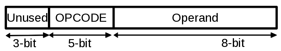
figure 1
- We would like to cover the following functionalities in our CPU:
- Addition/Subtraction
- Increment/Decrement
- Arithmetic and Logical Shift
- Bitwise AND, OR and XOR
- Negation
- Load/Store
- Unconditional Branch (jump)
- Branch if zero / Branch if Overflow
- Clear Registers/Flags
- NOP/HALT
- Your Pico-CPU's DataPath Unit, should have an accumulator register
which we call AC. The results of our operations will be written back
to AC after ALU calculation. You MAY have one more register in
your DPU which is transparent to programmer but its not obligatory
to have this register.
- There is no restrictions on how you implement the functionalities that
are required. As an example, you can do subtraction by combining
negation and addition. and there are lots of different approaches that
you can take, And its totally up to you.
- Important: In our design we dont implement relative or indexed
addressing. Only direct addressing is used.
Important: You MUST fill table 2 with your designed instruction set. We will collect these tables
at the beginning of exercise session. Students who do not bring the instruction set table to the lab, will not be allowed to start the exercise.
Draw Block diagram of your design
In this section we need you to draw the basic block diagram of your design
based on the design requirements of the previous section. we need the following
diagrams to be presented when you come to the lab: (not only the
wires but the direction of flow of data should be drawn)
- Draw the connections for Top level block diagram in figure 2.
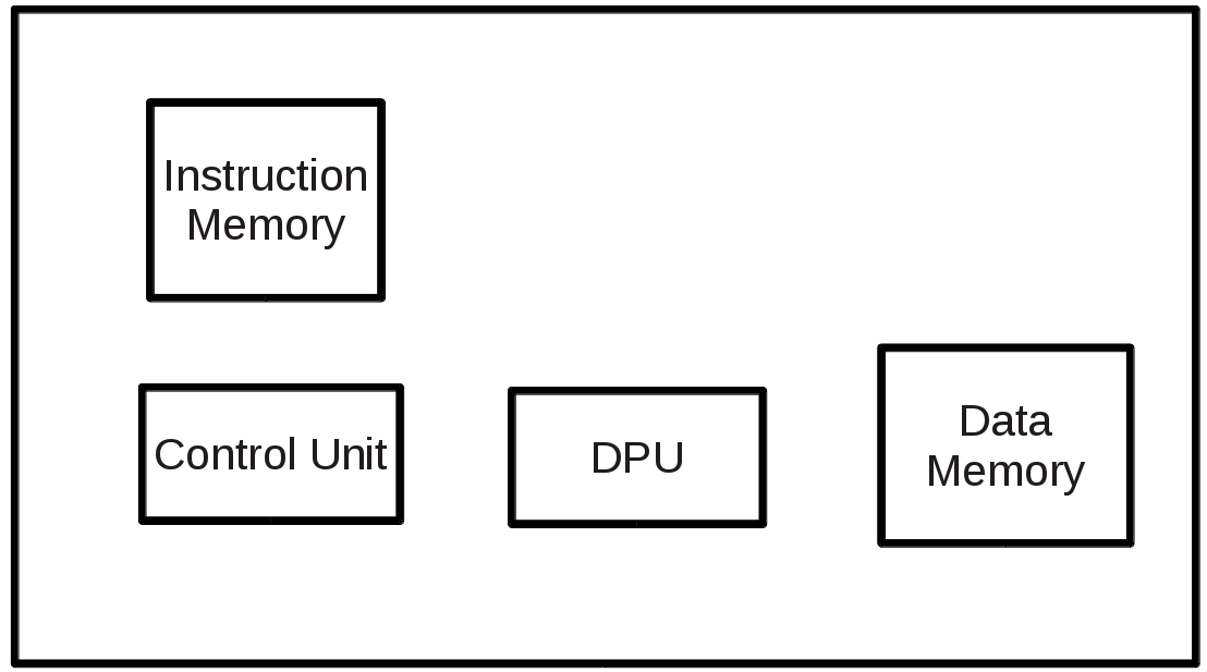
figure 2
- Draw the connections for Control unit block diagram in figure 3.

figure 3
- Draw the connections for DataPath unit block diagram in figure 4
(Note: you can either use or bypass the Register in Datapath).
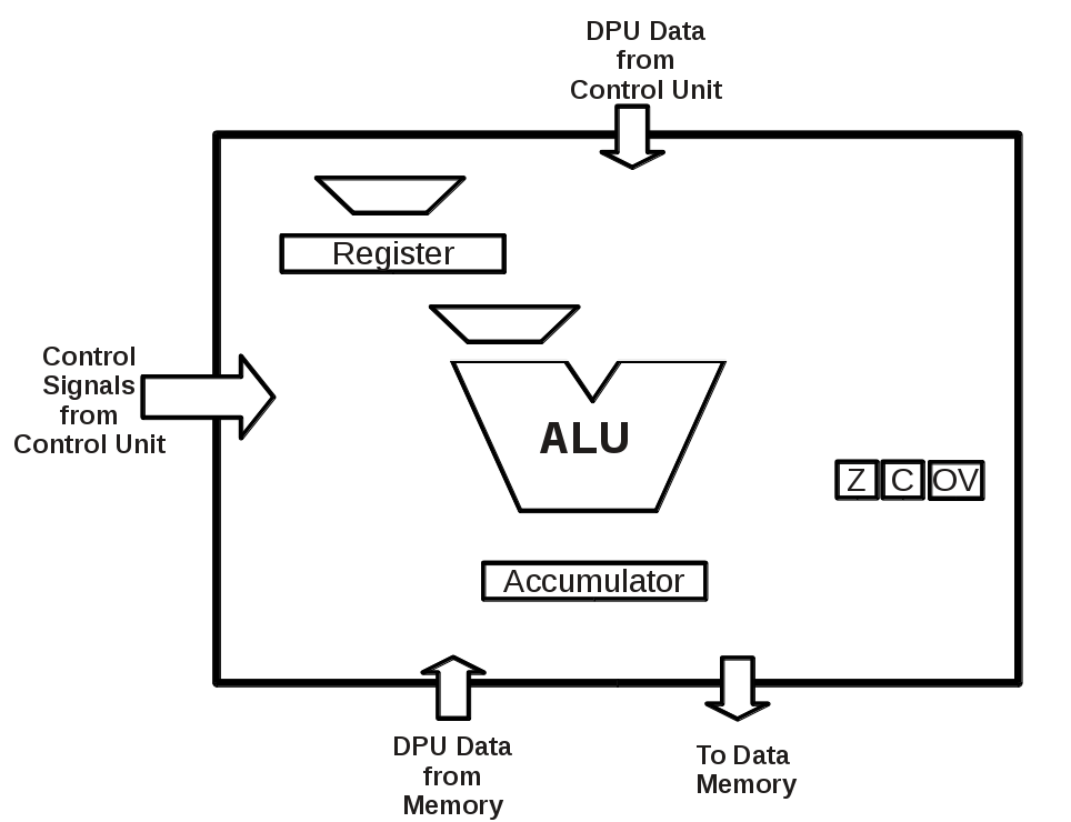
figure 4
Questions
- How much do you think you can compress the instruction set (in other words, what
is the lower bound on the number of instructions)?
- How will fewer and more simplistic instructions will effect programming
at user end? give an illustrative example that removing one
instruction will effect the code.
- What will be the effect of reducing the number of instruction on hard-
ware side?
- What will you personally prefer to have, larger instruction set or
smaller one? and why?
- How will you implement a multiplication operation with your proposed
instruction set?
- How can you implement delays with your proposed instruction set?
Related Readings