Counter, Adder
Tasks
- Download the VHDL code for Counter.vhd, Counter.ucf, adder.vhd and counter_tb.vhd.
- Create new Project in Xilinx ISE and Import downloaded files into the project.
- Open adder.vhd file. As you can see, this module has inputs and outputs of a full adder. But it only has one XOR gate implemented in it. Complete the boolean equations for a full adder as shown in figure 2. The full adder has three one bit wide data inputs: a, b,
and cin (carry-in); and two one bit wide outputs: sum and cout (carry-out). The sum output is the least significant bit (bit 0) of the sum of the three inputs.
The cout output is the most significant bit (bit 1) of the sum of the three inputs.
Full Adder truth table A B Cin S Cout 0 0 0 0 0 1 0 0 1 0 0 1 0 1 0 1 1 0 0 1 0 0 1 1 0 1 0 1 0 1 0 1 1 0 1 1 1 1 1 1 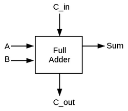 figure 1: Full Adder Interface
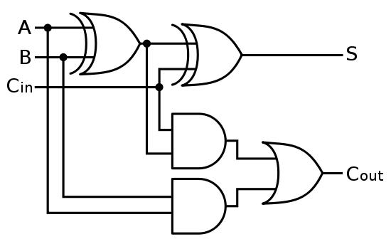 figure 2: Full Adder Schematic
 - As you can see there are a few things missing in
- In the adder write the equations for the full adder that you've made in task 1.
- Instanciate the adder into the counter using generate statment (for all bits of counter). An example for four bit ripple carry adder is shown in figure 3.

- Synthesize the provided design and fix the errors and warnings. Once the design is error free then read the synthesis report and program the board with the right tool. report Report area and Critical path .
- Convert the counter into an up/down counter and make sure it runs on the board.
- Add a new signal named up_down
- change the adder into a adder/subtractor
- connect adder subtract select signal to up_down
- synthesize
- Report area and critical path . Explain why they are different from 6b.
Related Readings