During this lab you're going to model NAND gate in SPICE (Simulation Program with Integrated Circuit Emphasis) language. To do this we use eldorado simulator from Mentor Graphics. NAND model should be done for 180 nm technology such a way that positive slope and negative slope would be equal for the output signal. To achieve this you should change the width of the transistor. The length of the transistors must be 180 nm.
You should simulate your model in eldorado simulator from Mentor Graphics. In order to compile the files you need to:
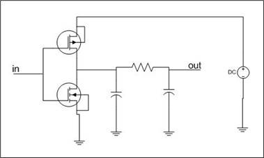
In order to practice using these tools a model of an inverter with wire connector to the inverter's output is given to you. On the Figure 1. is the schematic of the design.

Figure 1. Schematic picture of the inverter with wire at the output.
For this model PMOS and NMOS transistors of 180 nm technology are used, therefore length of a transistor is 180 nm. However width is at least 2 times bigger and the smallest equals to 360 nm. For wire model we have wire width of 2*180 nm = 360 nm. The length of the wire is 10 µm so we get resistance of 2,2 Ω and capacity of 2fF. The model written in SPICE is given to you in invWire.cir file. Note the different widths of NMOS and PMOS transistors (for explanation, see hints below). This model uses a subcircuit wire model which is given in wire.cir.
Firstly compile wire.cir and then invWire.cir. To use the subcircuit in your modules use the following SPICE
syntax:
X[name] [connections] [name of subcircuit]
Also you need to include subcircuit file itself with: .INCLUDE [file name]
In order to find the ratio of width between NMOS and PMOS transistors they could be approximated as resistors. In this case R ~ µ-1, where µ is mobility. For NMOS µn = 1250 cm2/V·s. For PMOS µp = 480 cm2/V·s. To find the correct ratio take the R ~ L/W as a reference. When taking account both mobility and size then R ~ L/(W·µ).
To describe MOS transistor in SPICE you need to declare it in the following format:
M[name] [drain node] [gate node] [source node] [bulk/substrate node] [model node] [model parameters
(length L, width W)]
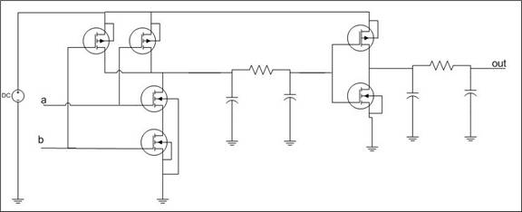
On Figure 2 is the schematic of the NAND.

Figure 2. Schematic of the NAND.
Figure 3. Solution of the NAND.