Important Note:
Please make sure you read Jiri Gaisler's "A structured VHDL design method". This document would be used as our coding reference throughout the labs.Format of Exercises
Before coming into the exercise sessions, students are required to understand prerequisites for each session. When the students arrive in the laboratory, they can be tested for following concepts for work,- A deep understanding of required concept of labs as explained in pre-requisite sessions of each exercise manual on the course website
- Written solution of problems given in pre-requisite section
- Softcopy of codes/scripts which students might need for the rest of the tasks
Tools user guides and manuals
You can find the user guides and manuals for these labs here: One will be tested for these concepts. The list of all the required concepts will be given as part of the exercise session.Simulation: multiplexer code modification
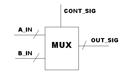
Task description: The purpose of this task is to become acquainted with simulation tool ModelSim.To get familiar with a VHDL files mux.vhd and mux_tb.vhd which are offered to you. Mux.vhd file is design file of multiplexer, which behavior is presented in Table 1. If the control signal CONT_SIG is '1' then the input A_IN is propagated to the output OUT_SIG, if the CONT_SIG is '0' then input B_IN is propagated to the output. The schematic of multiplexer is on Figure 1. Also testbench for the multiplexer is available in the mux_tb.vhd. The idea of the testbench is to test the behavioral design in simulation by forcing input signals and observe output values.| CONT_SIG value | OUT_SIG value |
| 1 | A_IN |
| 0 | B_IN |
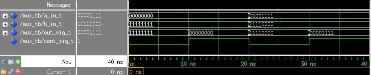
Simulation example
Tasks
- Take the guide for ModelSim simulator
and try to compile first design file mux.vhd.
Also take the testbench file mux_tb.vhd. Simulate the design and check the behavior.
- Design mux.vhd contains errors. Fix the errors and make sure that the behavior of the design is correct.
- Repeat the simulations using: Xilinx ISE guide.
- Change the code so that instead of sensitivity list the process uses wait command. Make sure the code is correct by simulation. Choose a
simulator you like best (ISE or ModelSim).
- Answer the questions.
- Continue with the Counter exercise.
Questions
- Explain the errors.
- What is the difference of entity and architecture?
- Can one entity have more than one architecture? Explain.
- Is it possible to get right waveforms of the signals during the
simulation, even when your design contains behavioral errors? Give
an example based on the lab.
Synthesis : Counter exercise for Blinking LED
Task description: The aim of this exercise is to understand how the flow of synthesis works. For this exercise following files are provided.
Consider a counter as shown in the figure .
- counter.vhd: has the vhdl code for a 32 counter
- counter_tb.vhd: has the testbench to test the counter
- counter.ucf: has the pin configuration which are needed by the FPGA board.
But the values are wrong. You have to change them to correct values before implementation otherwise
it will destroy the board. Determine the input and output pins.
You are expected to learn how to synthesize a peice of code on an FPGA. You will learn how to do pin assignments on a FPGA. The
counter used in this excercise has following signals:
- One bit input signal to reset the counter
- One bit input signal to enable the counter
- One bit input signal for the clock
- 32 bit internal signal for counter (which is not an I/O signal and hence will not be mentioned in UCF file).
- 1 bit output signal for blinking the LED
The UCF file only deals with Inputs and outputs description of the signals is explained in Table 2.
Simulate the counter and try to understand the code. The choice of the simulator is free.

Figure 1: Counter
with enable and reset
Table 2: Counter I/O
Signal
Type
Description
clk
input
Clock signal. Counter counts on the rising edge of the clock signal.
rstr_n
input
When '0' then resets the counter to zero
ENABLE
input
If the enable signal is 1, counter is counting up, Otherwise counter is stopped.
LED
output
Represents the current output value of the counter (31st bit).
Assume that the counter is functionally verified so you can go straight to synthesis.
Tasks
- Create a new Project in Xilinx ISE and import the given VHDL files for counter. (counter.vhd, counter_tb.vhd, counter.ucf) A refrence guide on how to make a project is available here.
- Make a UCF file such that enable is connected to FPGA switches, rst_n is connected to button switch, led is connected to LED of the board and clk is connected to the clock pin of the FPGA board.
To figure out what should be the correct pin use the NEXYS2 user manual . Specially look at page 4 and page 5. OR
FPGA manual for Digilent Spartan 3E stater page 15,16, 19 and 20.
- You are free to choose any of the button, switches and LEDs available on the board. Change the properties of the project and change the family, device and package based on the board. HINT: look at the chip titled Xilinx.
- Synthesize the design
- As it can be seen there are a few warning. Resolve them by
entering the correct signal in the sensitivity list. led signal needs to be assigned, assign the 24th bit of counter to it.
- Synthesize the design again, you will see few more warnings. This is because the bits of counter beyond the led output have no use and the synthesis tool realizes it. Change the dimentions of the counter to fix it.
- Once all the warnings are eliminated then implement the design.
- Before generating the bit file go right click on "Generate Programming File → Process Properties → Startup Options → Change FPGA startup clock to JTAG Clock.
- Generate the programming File (bit file). The process window in ise will look like the following screen shot. Then you will need to write the bitfile (counter.bit) into the FPGA using this guide.
 Figure 2: screenshot of finished implementation
- Read the
FPGA manual for nexy2 specially look at the figure 8 (in the manual) or
FPGA manual for Digilent Spartan 3E stater page 15,16, 19 and 20, to see how the buttons work. Now open the counter code and look at rst_n signal.
- Will the counter reset when the button is pressed?
- if yes, then press the button while the enable switch is on and explain the behaviour?
- if no, what should be changed to fix it?
- what is the clock frequency of the FPGA. Now change the vhdl code for counter.vhd which assigns led to look as follows
led <= counter(22);
- Save the changes and repeat steps from 6 onwards. And try to answer
the following questions.
- why did the LED frequency change?
- Can we make the LED blink Every one second?
- if yes, then why change should we do to the code to achieve it?
- if no, why? then what is the closest frequency to the requirement.
- Defend the lab orally and write a report. Requirements can be found here .
The report must include both exercises (multiplexer and counter).
- Explain the errors.
- What is the difference of entity and architecture?
- Can one entity have more than one architecture? Explain.
- Is it possible to get right waveforms of the signals during the simulation, even when your design contains behavioral errors? Give an example based on the lab.
Synthesis : Counter exercise for Blinking LED
Task description: The aim of this exercise is to understand how the flow of synthesis works. For this exercise following files are provided. Consider a counter as shown in the figure .- counter.vhd: has the vhdl code for a 32 counter
- counter_tb.vhd: has the testbench to test the counter
- counter.ucf: has the pin configuration which are needed by the FPGA board. But the values are wrong. You have to change them to correct values before implementation otherwise it will destroy the board. Determine the input and output pins.
- counter_tb.vhd: has the testbench to test the counter
- One bit input signal to reset the counter
- One bit input signal to enable the counter
- One bit input signal for the clock
- 32 bit internal signal for counter (which is not an I/O signal and hence will not be mentioned in UCF file).
- 1 bit output signal for blinking the LED
Figure 1: Counter
with enable and reset
| Signal | Type | Description |
| clk | input | Clock signal. Counter counts on the rising edge of the clock signal. |
| rstr_n | input | When '0' then resets the counter to zero |
| ENABLE | input | If the enable signal is 1, counter is counting up, Otherwise counter is stopped. |
| LED | output | Represents the current output value of the counter (31st bit). |
Tasks
- Create a new Project in Xilinx ISE and import the given VHDL files for counter. (counter.vhd, counter_tb.vhd, counter.ucf) A refrence guide on how to make a project is available here.
- Make a UCF file such that enable is connected to FPGA switches, rst_n is connected to button switch, led is connected to LED of the board and clk is connected to the clock pin of the FPGA board. To figure out what should be the correct pin use the NEXYS2 user manual . Specially look at page 4 and page 5. OR FPGA manual for Digilent Spartan 3E stater page 15,16, 19 and 20.
- You are free to choose any of the button, switches and LEDs available on the board. Change the properties of the project and change the family, device and package based on the board. HINT: look at the chip titled Xilinx.
- Synthesize the design
- As it can be seen there are a few warning. Resolve them by entering the correct signal in the sensitivity list. led signal needs to be assigned, assign the 24th bit of counter to it.
- Synthesize the design again, you will see few more warnings. This is because the bits of counter beyond the led output have no use and the synthesis tool realizes it. Change the dimentions of the counter to fix it.
- Once all the warnings are eliminated then implement the design.
- Before generating the bit file go right click on "Generate Programming File → Process Properties → Startup Options → Change FPGA startup clock to JTAG Clock.
- Generate the programming File (bit file). The process window in ise will look like the following screen shot. Then you will need to write the bitfile (counter.bit) into the FPGA using this guide.
Figure 2: screenshot of finished implementation
- Read the FPGA manual for nexy2 specially look at the figure 8 (in the manual) or FPGA manual for Digilent Spartan 3E stater page 15,16, 19 and 20, to see how the buttons work. Now open the counter code and look at rst_n signal.
- Will the counter reset when the button is pressed?
- if yes, then press the button while the enable switch is on and explain the behaviour?
- if no, what should be changed to fix it?
- what is the clock frequency of the FPGA. Now change the vhdl code for counter.vhd which assigns led to look as follows
led <= counter(22);- Save the changes and repeat steps from 6 onwards. And try to answer the following questions.
- why did the LED frequency change?
- Can we make the LED blink Every one second?
- if yes, then why change should we do to the code to achieve it?
- if no, why? then what is the closest frequency to the requirement.
- Defend the lab orally and write a report. Requirements can be found here . The report must include both exercises (multiplexer and counter).
- Make a UCF file such that enable is connected to FPGA switches, rst_n is connected to button switch, led is connected to LED of the board and clk is connected to the clock pin of the FPGA board. To figure out what should be the correct pin use the NEXYS2 user manual . Specially look at page 4 and page 5. OR FPGA manual for Digilent Spartan 3E stater page 15,16, 19 and 20.