Important Note:
Please make sure you read Jiri Gaisler's "A structured VHDL design method". This document would be used as our coding reference throughout the labs.Format of Exercises
Before coming into the exercise sessions, students are required to understand prerequisites for each session. When the students arrive in the laboratory, they can be tested for following concepts for work,- A deep understanding of required concept of labs as explained in pre-requisite sessions of each exercise manual on the course website
- Written solution of problems given in pre-requisite section
- Softcopy of codes/scripts which students might need for the rest of the tasks
Tools user guides and manuals
You can find the user guides and manuals for these labs here: One will be tested for these concepts. The list of all the required concepts will be given as part of the exercise session.Pre-Requisite
Students are supposed to revise their gate level structure of Adders, subtractors and binary counters. Students are expected to complete exercises given in compendium #1. In the beginning of the session students will be asked to give a written test from the compendium. If the student fails to pass complete the assignment he/she will be asked to submit a written version of the solution for the complete compendium before starting the exercise.Task description
The purpose of this task is to model basic elements of digital logic design and use them on an FPGA. and understand different abstractions and styles of coding We will start with lab counter similar example which was used in the first exercise. But in this example the added code is partitioned. This is because we wish to issolate the adder and experiment on this part of the code. Currently the code is written in register transfer level(RTL). we will convert this code into different levels of abstraction and using different styles of codes.Task
- Download the VHDL code for Counter.vhd,Counter.ucf,adder.vhd and counter_tb.vhd.
- Create new Project in Xilinx ISE and Import downloaded files into the project.
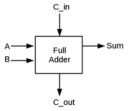
- Open adder.vhd file. As you can see, this module has inputs and outputs of a full adder. But it only has one XOR gate implemented in it. Complete the boolean equations for a full adder as shown in figure 2. The full adder has three one bit wide data inputs: a, b,
and cin (carry-in); and two one bit wide outputs: sum and cout (carry-out). The sum output is the least significant bit (bit 0) of the sum of the three inputs.
The cout output is the most significant bit (bit 1) of the sum of the three inputs.
Full Adder truth table A B Cin S Cout 0 0 0 0 0 1 0 0 1 0 0 1 0 1 0 1 1 0 0 1 0 0 1 1 0 1 0 1 0 1 0 1 1 0 1 1 1 1 1 1  figure 1: Full Adder Interface
 figure 2: Full Adder Schematic
 - As you can see there are a few things missing in
- In the adder write the equations for the full adder that you've made in task 1.
- Instanciate the adder into the counter using generate statment (for all bits of counter). An example for four bit ripple carry adder is shown in figure 3.

- Synthesize the provided design and fix the errors and warnings. Once the design is error free then read the synthesis report and program the board with the right tool.
- Report area
- Critical path
- Convert the counter into an up/down counter and make sure it runs on the board.
- Add a new signal named up_down
- change the adder into a adder/subtractor
- connect adder subtract select signal to up_down
- synthesize
- Report area and critical path . Explain why they are different from 6b.