Important Note:
Please make sure you read Jiri Gaisler's "A structured VHDL design method". This document would be used as our coding reference throughout the labs.Format of Exercises
Before coming into the exercise sessions, students are required to understand prerequisites for each session. When the students arrive in the laboratory, they can be tested for following concepts for work,- A deep understanding of required concept of labs as explained in per-Requisite sessions of each exercise manual on the course website
- Written solution of problems given in Pr-requisite section
- Softcopy of codes/scripts which students might need for the rest of the tasks
Tools user guides and manuals
You can find the user guides and manuals for these labs here:Task description
In this section you will be shown how to model a shift register properly as well as how to make registers and wires properly. Consider an example of shift register given in Figure 1. This requires a serial input which is shifter at every clock cycle. we will use this example to understand how to design shift register properly.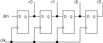
figure 1
For this lab you will need following set of codes
- shr1_tb.vhd test bench for the shift register in tast 1
- shr1.vhd shift register in task 1
- shr2.vhd shift register in tast 2
- shr2_tb.vhd test bench for the shift register task 2
Tasks
- Download the shift register files, read shr1.vhd and simulate it using the provided testbench shr1_tb.vhd.
- As it can be seen from the simulation that it is behaving as a wire rather then a register. This is because it lacks a clocked body.
- Add clk signal in the process sentitiveity list
- Add the contents of the body of the process p_shr in a if condition which works on the case "rising_edge(clk)". This will convert all the signal assignments into registers.
- simulate the design again. and check if it behaves as a shift register now?
- as you can see it still does not behave as a shift register. Explain why?
- Make the required change to the process and simulate it. verify if the code simulate
- Download the shift register files, read shr2.vhd, shr2_tb.vhd.
- As it can be seen from simulation, this shift register shifts a value everytime the enable signal goes from zero to one. Synthesize it using ISE and connect enable signal to one of the button on the FPGA.
- make a UCF file binding enable signal with the Button pin(see FPGA manual for the correct pin).
- synthesize and map it to the FPGA.
- Test if it works properly. Explain why the shifter jumps multiple times in reality while it skips once in simulation.
- Build a debounching circuit
- Reuse the fixed Shift Register in example one to build the debouncing circuit. as shown in the following diagram
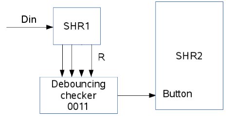 figure 1
 - Test if it works.
- no? make the shift register wider and try again
- yes, explained what happened here.
- Reuse the fixed Shift Register in example one to build the debouncing circuit. as shown in the following diagram