Difference between revisions of "CDS LAB1/en"
From ATI public wiki
(starting translation (by SublimeText.Mediawiker)) |
((by SublimeText.Mediawiker)) |
||
| (8 intermediate revisions by the same user not shown) | |||
| Line 1: | Line 1: | ||
| + | [[CDS_LAB1|Eesti keelne leht]] [[File:Estonia.png | 32px | link=CDS_LAB1]] | ||
| + | |||
| + | |||
<big>The objective of the tutorial is to design a digital circuit and simulate it using Cadence</big> | <big>The objective of the tutorial is to design a digital circuit and simulate it using Cadence</big> | ||
| Line 16: | Line 19: | ||
:* If it is the first time launching Cadence, then using terminal: | :* If it is the first time launching Cadence, then using terminal: | ||
:: <pre>ams_cds -64 -tech c18a6 -add CORELIB -add IOLIB_6AM -add GATES_ANA</pre> | :: <pre>ams_cds -64 -tech c18a6 -add CORELIB -add IOLIB_6AM -add GATES_ANA</pre> | ||
| + | :: here we choose AMS 0.18μm with 6 metal layers as the technology and add three gate libraries | ||
| + | :* For the subsequent launches of Cadence use the command: | ||
| + | :: <pre>ams_cds</pre> | ||
| + | |||
| + | :[[File:Cds lab1 2.png|Launching Cadence]] | ||
| + | |||
| + | : ''The actions from this point on will be executed using the Graphical User Interface of Cadence'' | ||
| + | |||
| + | : Several windows will open. On a dialog window asking about ''designkit'' simply press ''OK''. | ||
| + | :[[File:Cds lab1 3.png|Designkit dialog]] | ||
| + | |||
| + | |||
| + | : Cadence main window will be also opening, which is located by default near the left bottom corner. | ||
| + | :[[File:Cds lab1 4.png|Cadence main window]] | ||
| + | : Cadence will log messages in this window, including error messages. | ||
| + | |||
| + | : Also Cadence Library Manager window will open | ||
| + | :[[File:Cds lab1 5.png|Library Manager]] | ||
| + | : It is recommended to check the checkbox '''Show Categories''' | ||
| + | |||
| + | ==Creating a new library== | ||
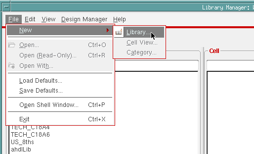
| + | : In the Library Manager window choose from menu '''File->New->Library''' | ||
| + | :[[File:Cds lab1 6.png|Loome uue library]] | ||
| + | |||
| + | |||
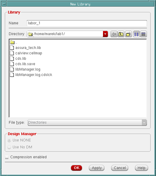
| + | : A new window will open, where a name can be inserted. In here '''labor_1''' will be used. After inserting the name, press '''OK''' | ||
| + | :[[File:Cds lab1 7.png|Loome uue library]] | ||
| + | |||
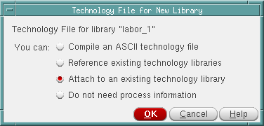
| + | : Another window will appear with couple of choices. Choose '''Attach to an existing technology library''' and press '''OK''' | ||
| + | :[[File:Cds lab1 8.png|new library technology]] | ||
| + | |||
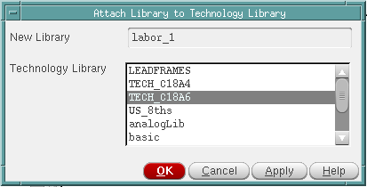
| + | : In the next window choose '''TECH_C18A6''' and press '''OK''' | ||
| + | :[[File:Cds lab1 9.png|new library technology]] | ||
| + | |||
| + | ==Creating new circuit into our library== | ||
| + | : Choose the newly created library '''labor_1''' in the '''Library Manager''' window. In the menu choose '''File->New->Cell View''' | ||
| + | :[[File:Cds lab1 10.png|creating new cell]] | ||
| + | |||
| + | |||
| + | |||
| + | : In the window opened fill the field '''Cell''' by giving your new circuit a name, e.g. '''half_adder'''. On the images below ''poolsummaator'' is used as the name. | ||
| + | :[[File:Cds lab1 11.png|creating new cell]] | ||
| + | : Choose '''Applications->Schematics XL''' and select checkbox '''Always use this application for this type of file''' and press '''OK'''. As a result the schematic editor window will open. | ||
| + | |||
| + | |||
| + | == Editing the half-adder schematic == | ||
| + | |||
| + | : As a result of the previous actions we should have a schematic editor window open. | ||
| + | :[[File:Cds lab1 12.png|Cadence schematic editor]] | ||
| + | |||
| + | |||
| + | : Overview of some of the schematic shortcuts | ||
| + | :* ''''i'''' - '''''instance''''' , adding new instance of a cell to the schematic | ||
| + | :* ''''w'''' - '''''wire''''' , adding wire to the schematic for connecting elements | ||
| + | :* ''''l'''' - '''''label''''' , inserting a label on a connection | ||
| + | :* ''''p'''' - '''''pin''''' , creating a new input/output pin | ||
| + | :* ''''f'''' - '''''fit to view''''' , changes to zoom to fit the whole schematic to the view | ||
| + | :* ''''u'''' - '''''undo''''' , undo the last action | ||
| + | :* ''''X'''' - '''''Check and Save'''' , checks the schematic and saves it | ||
| + | |||
| + | |||
| + | :: Zooming in can be done by holding down the right mouse button and selecting an area. To leave the zoom quickly, press '''f''' | ||
| + | :: From every insertion mode you can quickly exit by pressing '''ESC''' | ||
| + | :: When in the '''wire''' mode, you can press '''s''' for snap functionality. | ||
| + | :: '''NB!''' Undo works until last save. Changes made before the save can not be taken back. | ||
| + | |||
| + | ===Creating a sheet border and title=== | ||
| + | : Press the key '''i''' and in the opening window press '''Browse''' | ||
| + | :[[File:Cds lab1 13.png|Cadence add instance window]] | ||
| + | : '''Library Browser''' will open where you should navigate to '''Library->BORDERS->Cell->A5'''. | ||
| + | : We can close the '''Library Manager''' window by pressing '''Close''' | ||
| + | : Also we can hide the '''Add Instance''' window temporarily by pressing '''Hide''' | ||
| + | |||
| + | : After that the border can be placed by moving mouse in the black area of schematic editor and pressing left mouse button. | ||
| + | :[[File:Cds lab1 14.png|Cadence schematic editor]] | ||
| + | : When the border is placed, you can press '''f''' to ''fit the view''. | ||
| + | |||
| + | ===Adding schematic elemenets of half-adder=== | ||
| + | : Press the key '''i''' and choose '''Browse''' | ||
| + | : In the '''Library Browser''' window that opened, navigate to '''Library->CORELIB''' where the schematic elements can be found. | ||
| + | |||
| + | |||
| + | : First of all we need to place some AND gates. | ||
| + | :[[File:Cds lab1 15.png|Cadence Library Manager, AND element]] | ||
| + | : To do that, navigate to '''Category->AND->Cell->AND2X1''' | ||
| + | : The numbers after the gate name show how many inputs does it have and its fan-out (number of gate inputs it can feed or connect to). In this case we have a two input AND gate with 1 fan-out. | ||
| + | |||
| + | |||
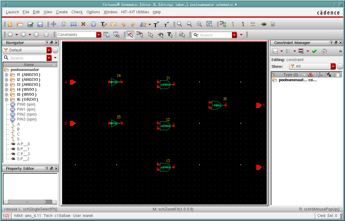
| + | : For a half-adder we need 3 AND gates, 2 NOT gates (inverters) and 1 OR gate | ||
| + | :[[File:Cds lab1 16.png|Cadence schematic editor, half-adder gates]] | ||
| + | |||
| + | ===Adding inputs and outputs for the half-adder=== | ||
| + | : To add the inputs and output pins, press '''p''' | ||
| + | :[[File:Cds lab1 17.png|Cadence schematic editor, adding inputs]] | ||
| + | : For the first pin name choose '''A''' with direction '''input''' | ||
| + | : Placing pins works the same way as placing instances of cells | ||
| + | |||
| + | |||
| + | : For a half-adder we need two inputs (A and B) and two outputs (Sum and Carry) | ||
| + | :[[File:Cds lab1 18.png|Cadence schematic editor, with inputs]] | ||
| + | |||
| + | |||
| + | ===Adding connections=== | ||
| + | : Press '''w''' to choose wire and by using ''snap'', connect the elements as following: | ||
| + | :[[File:Cds lab1 19.png|Cadence schematic editor, half-adder connections]] | ||
| + | : For a better readability of the schematic you can add labels by pressing the key '''l'''. | ||
| + | |||
| + | |||
| + | ===Saving the half-adder schematic=== | ||
| + | : For saving the schematic press '''x''' | ||
| + | :[[File:Cds lab1 20.png|Cadence põhiaken, check-and-save]] | ||
| + | : In the Cadence main window you can check whether the saving was successful and if not, what were the errors. | ||
| + | |||
| + | ===Creating a symbol for the half-adder=== | ||
| + | : In order to use the newly created schematic as a component in other schematics, a '''symbol''' view must be created. | ||
| + | :[[File:Cds lab1 21.png|Cadence Skeemiredaktor]] | ||
| + | : To create a symbol, navigate from menu to '''Create->Cellview->From Cellview''' | ||
| + | |||
| + | :[[File:Cds lab1 22.png|Cellview from Cellview]] | ||
| + | : A window will pop up, where you can simply press '''OK''' as the default options are fine at this point. | ||
| + | |||
| + | :[[File:Cds lab1 23.png|Symbol Generation Options]] | ||
| + | : In the following popup window you can choose the pin specifications. | ||
| + | : Finally continue by pressing '''OK''' | ||
| + | |||
| + | : Next, '''Cadence Symbol Editor''' will open | ||
| + | :[[File:Cds lab1 24.png|Cadence Symbol Editor]] | ||
| + | : The symbol created by default is a rectable. By using the toolbar, it can be designed as desired. | ||
| + | |||
| + | == Full adder from two half-adders == | ||
| + | |||
| + | : By using the finished half-adder component, we can create a full adder | ||
| + | :[[File:Cds lab1 25.png|Cadence Schematic Editor]] | ||
| + | : This can be made into a symbol as well, so it can be used in other schematics as a component. | ||
| + | |||
| + | : The component can be also be opened in schematic view. To do that: | ||
| + | :* Double click on the component symbol | ||
| + | :* Use the command '''Descend Edit''' or its shortcut '''Shift+E''' | ||
| + | : To return back to last view '''Return''' command can be used or its shortcut '''Ctrl+E''' | ||
| + | |||
| + | : This can be useful for example when we need to change the fanout of the component. | ||
| + | |||
| + | : '''NB!''' when changing the component, it will change everywhere, where it has been used. | ||
| + | |||
| + | |||
| + | ==4-bit adder== | ||
| + | |||
| + | : Now we should have all the components necessary for a 4-bit adder: one half-adder and three full-adders. | ||
| + | |||
| + | : Carry chain can be done serially in this schematic with '''Ripple Carry Adder''', which is suitable for a small 4-bit adder. For bigger adders parallel carry would be recommended, e.g. '''Lynch-Swartzlander Spanning Tree Carry Lookahead Adder'''. | ||
| + | |||
| + | : For this schematic we will be using 4-bit bus. | ||
| + | : To make the buses more visible, we will use bold line for the connections. | ||
| + | : For bringing out individual bits from a bus and connecting them, '''labelling must be used.''' | ||
| + | |||
| + | :[[File:Cds lab1 26.png|Cadence Schematic Editor, 4bit adder]] | ||
| + | |||
| + | ==4-bit adder simulation== | ||
| + | |||
| + | : Now that we have finished, checked and saved the schematic design, we will proceed with simulation. | ||
| + | : Let us open the tool '''NC-Verilog''' | ||
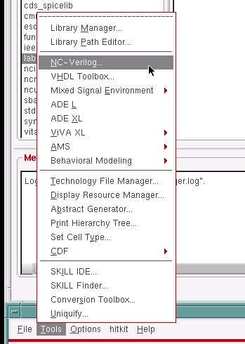
| + | : From Cadence main window choose from menu '''Tools->NC-Verilog''' | ||
| + | :[[File:Cds lab1 27.png|Cadence main window, Tools menu]] | ||
| + | |||
| + | |||
| + | : A new window will open where a few things should be configured | ||
| + | :[[File:Cds lab1 28.png|Cadence NC-Verilog window]] | ||
| + | :* '''Run Directory''' - press on the button with three dots (...) and choose a working directory. (In this case we should create the working directory, for example '''lab1_simu''') | ||
| + | ::[[File:Cds lab1 29.png|Cadence NC-Verilog window]] | ||
| + | :*Choose design by pressing on '''Browse''', selecting your schematic and '''schematic''' view. | ||
| + | |||
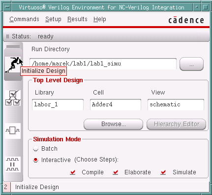
| + | ===NC-Verilog initialization and settings=== | ||
| + | |||
| + | :Press on the first icon in the left '''Initialize Design''' | ||
| + | :[[File:Cds lab1 30.png|Cadence NC-Verilog window]] | ||
| + | |||
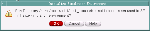
| + | :A window will pop up where '''OK''' should be chosen. | ||
| + | :[[File:Cds lab1 31.png|Cadence NC-Verilog window]] | ||
| + | |||
| + | |||
| + | :Configure a few parameters from '''Setup->Netlist''' | ||
| + | :[[File:Cds lab1 32.png|Cadence NC-Verilog window]] | ||
| + | |||
| + | :A menu will open | ||
| + | :[[File:Cds lab1 33.png|Cadence NC-Verilog Netlist Setup]] | ||
| + | :Choose the following settings | ||
| + | :* '''Netlist These Views->schematic symbol''' | ||
| + | :* choose '''Single Netlist File''' | ||
| + | :* '''Global Sim Time''' set as 1 with unit '''ps''' | ||
| + | :* '''Global Sim Precision''' set as 1 with unit '''fs''' | ||
| + | |||
| + | :Next, choose '''Setup->Record Signals''' | ||
| + | :[[File:Cds lab1 34.png|Cadence NC-Verilog Record Signals Setup]] | ||
| + | :Choose '''All''' | ||
| + | |||
| + | ===Creating NC-Verilog Netlist=== | ||
| + | |||
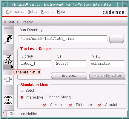
| + | :As a next step we should generate netlist for our schematic. For that press on the NC-Verilog main window a button '''Generate Netlist''' | ||
| + | :[[File:Cds lab1 35.png|Cadence NC-Verilog Generate Netlist]] | ||
| + | |||
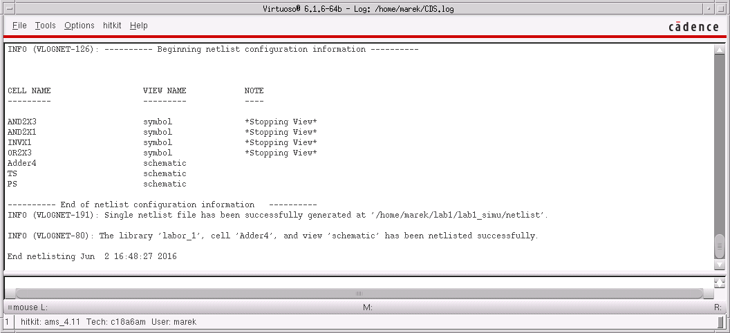
| + | : On the Cadence main window you can check whether the netlist was generated successfully without errors. | ||
| + | :[[File:Cds lab1 36.png|Cadence Main Window, netlist generation output]] | ||
| + | |||
| + | ===NC-Verilog simulation input data=== | ||
| + | |||
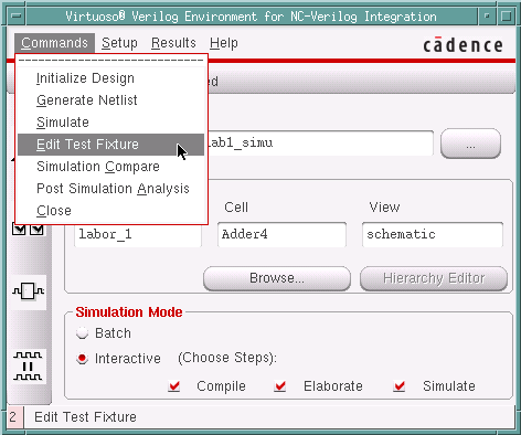
| + | :For the simulator to be able to simulate anything, we need input data | ||
| + | :For this purpose choose from NC-Verilog main window '''Commands->Edit Test Fixture''' | ||
| + | :[[File:Cds lab1 37.png|Cadence NC-Verilog Edit Test Fixture]] | ||
| + | |||
| + | |||
| + | :[[File:Cds lab1 38.png|Cadence NC-Verilog Edit Test Fixture]] | ||
| + | : In the opened window there are two panes: '''TestBench''' and '''Stimulus''' | ||
| + | : For a simple simulation, we are only interested in '''Stimulus''' section. Press there on the '''Edit''' button. | ||
| + | |||
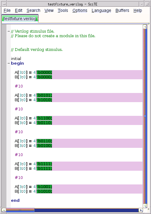
| + | : A text editor should open with a file '''testfixture.verilog''' | ||
| + | :[[File:Cds lab1 39.png|SciTE edit Test Fixture]] | ||
| + | : Here you can see code generated by default that initializes the simulation. | ||
| + | |||
| + | : Now we can add our own values. 4 to 5 input number pairs, every change simulate for 10 simulation units. | ||
| + | :[[File:Cds lab1 40.png|SciTE edit Test Fixture]] | ||
| + | |||
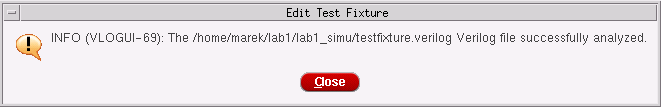
| + | : After editing, it is a good idea to check for errors. This can be done from '''Edit Test Fixture''' window with a button '''Check Syntax''' | ||
| + | : If everything is good, a message will be displayed | ||
| + | :[[File:Cds lab1 41.png|Edit Test Fixture Check Syntax]] | ||
| + | |||
| + | ===NC-Verilog Simulation=== | ||
| + | |||
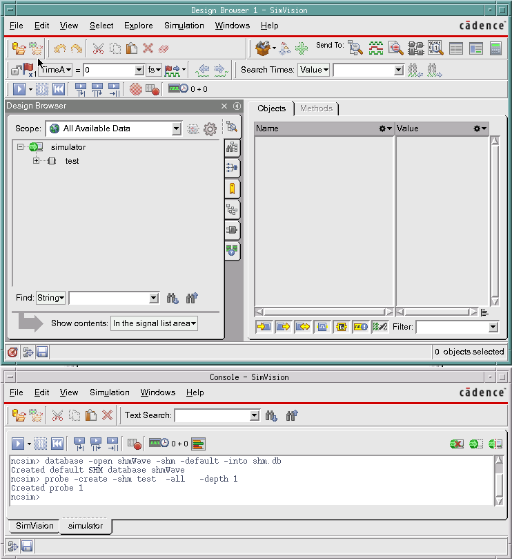
| + | : Start the simulation by clikcing in the '''NC-Verilog''' main window, on the left side on a button '''Simulate''' | ||
| + | : As a result '''SimVision''' will start and two new windows will open: '''Console - SimVision''' and '''Design Browser = SimVision''' | ||
| + | :[[File:Cds lab1 42.png|Cadence SimVision]] | ||
| + | |||
| + | |||
| + | ==Simulation results, SimVision== | ||
| + | |||
| + | ===Viewing simulation results=== | ||
| + | |||
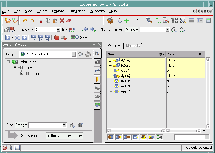
| + | : In the opened windows, let us focus on the '''Design Browser''' | ||
| + | |||
| + | :[[File:Cds lab1 43.png|Cadence SimVision Design Browser]] | ||
| + | : Here, on the left side of the window, choose '''-simulator-test+top''' | ||
| + | : and on the right side of the window choose inputs-outputs for which values we are interested of seeing on the waveform graph. Finally press on '''Send to Waveform'''. | ||
| + | |||
| + | :A new window will appear: '''Waveform - SimVision''' | ||
| + | :[[File:Cds lab1 44.png|Cadence SimVision Waveform]] | ||
| + | |||
| + | |||
| + | : Here, press on a triangle symbol by the Run button, so that we could edit time field. | ||
| + | : In the time field insert a number of simulation units, '''60'''. | ||
| + | : and press '''Run''' button. | ||
| + | :[[File:Cds lab1 45.png|Cadence SimVision Waveform, run run run]] | ||
| + | |||
| + | |||
| + | : So that we could see the whole view, the waveform should be zoomed out. Press <big>'''='''</big> button on the right border of the toolbar. | ||
| + | :[[File:Cds lab1 46.png|Cadence SimVision Waveform, zoooooooom]] | ||
| + | |||
| + | : If we have multiple outputs that are related with each other, in this case '''Carry''' signal and sum output, it is reasonable to view them together for a better readabilty. | ||
| + | : In order to do that simply copy these two signals - with left mouse button click on the signals while holding SHIFT key and then by clicking right mouse button, choose '''Copy''' from the menu. | ||
| + | :[[File:Cds lab1 47.png|Cadence SimVision Waveform, copy]] | ||
| + | : Finally paste the signals down below, by clicking again with the right mouse button on the black background and choose '''Paste''' | ||
| + | |||
| + | |||
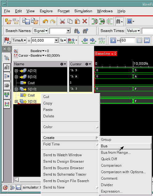
| + | :Afterwards choose the copied signals and by pressing again on the right mouse button choose '''Create->Bus''' from the menu. | ||
| + | :[[File:Cds lab1 48.png|Cadence SimVision Waveform, create bus]] | ||
| + | |||
| + | ===Simulation results=== | ||
| + | |||
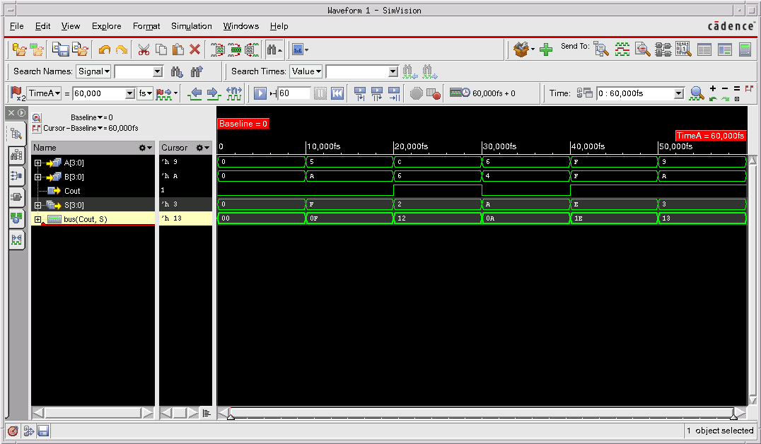
| + | : Now we can easily follow the waveform and check the results of the adder | ||
| + | :[[File:Cds lab1 49.png|Cadence SimVision Waveform, lõppvaatus]] | ||
Latest revision as of 17:48, 15 June 2016
The objective of the tutorial is to design a digital circuit and simulate it using Cadence
Contents
Setting up the work environment
All the actions in this and the followin paragprah will be happening in terminal
- create a new directory lab1
- move to the new directory
- insert 'cad' and from the menu choose '1' (initializes environmental variables for Cadence)
- insert setenv EDITOR SciTE for making SciTE as the default text editor

Starting Cadence
- According to Cadence 2016 EDA ver.
- If it is the first time launching Cadence, then using terminal:
-
ams_cds -64 -tech c18a6 -add CORELIB -add IOLIB_6AM -add GATES_ANA
- here we choose AMS 0.18μm with 6 metal layers as the technology and add three gate libraries
- For the subsequent launches of Cadence use the command:
-
ams_cds

- The actions from this point on will be executed using the Graphical User Interface of Cadence
- Several windows will open. On a dialog window asking about designkit simply press OK.

- Cadence main window will be also opening, which is located by default near the left bottom corner.
- Cadence will log messages in this window, including error messages.

- Also Cadence Library Manager window will open
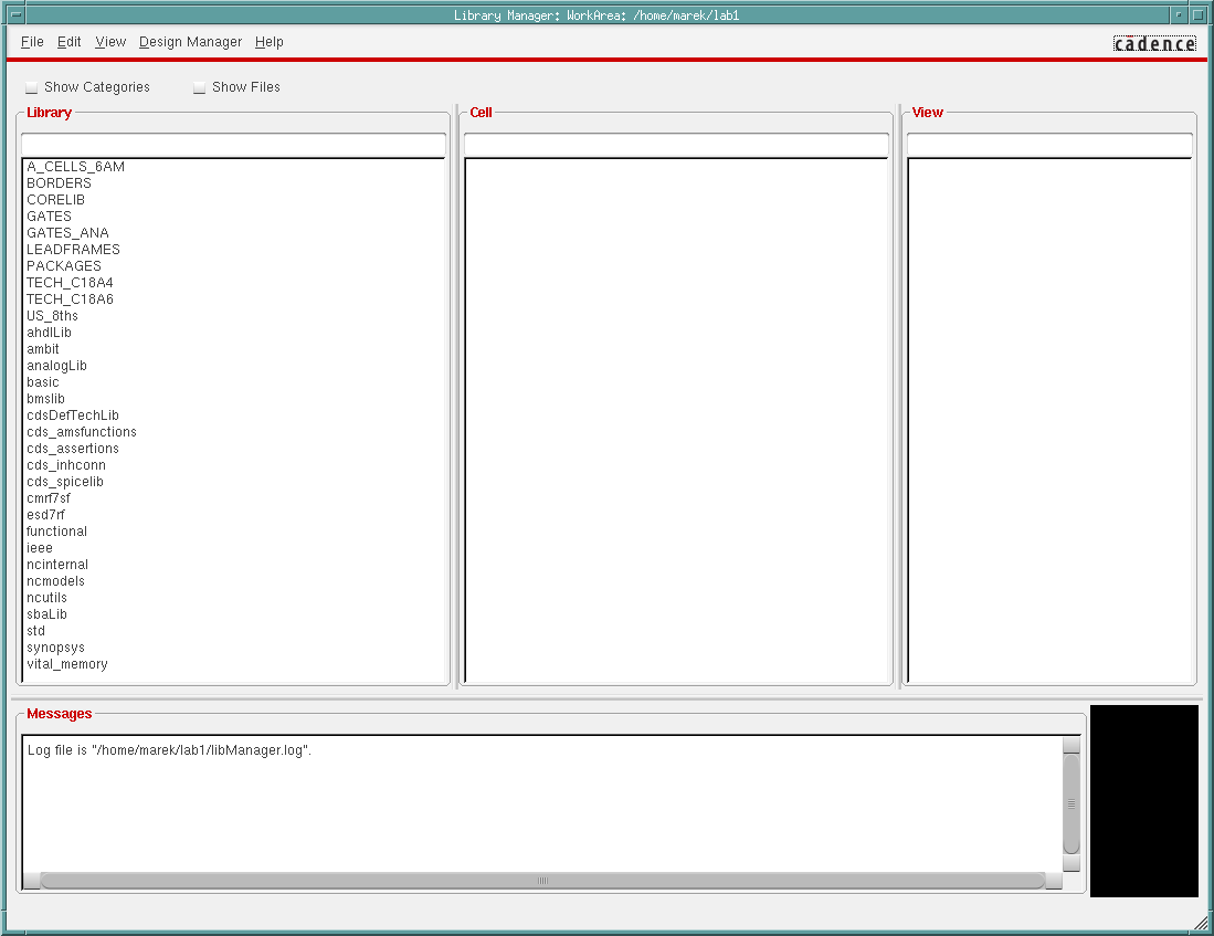
- It is recommended to check the checkbox Show Categories

Creating a new library
- In the Library Manager window choose from menu File->New->Library

- A new window will open, where a name can be inserted. In here labor_1 will be used. After inserting the name, press OK

- Another window will appear with couple of choices. Choose Attach to an existing technology library and press OK

- In the next window choose TECH_C18A6 and press OK

Creating new circuit into our library
- Choose the newly created library labor_1 in the Library Manager window. In the menu choose File->New->Cell View
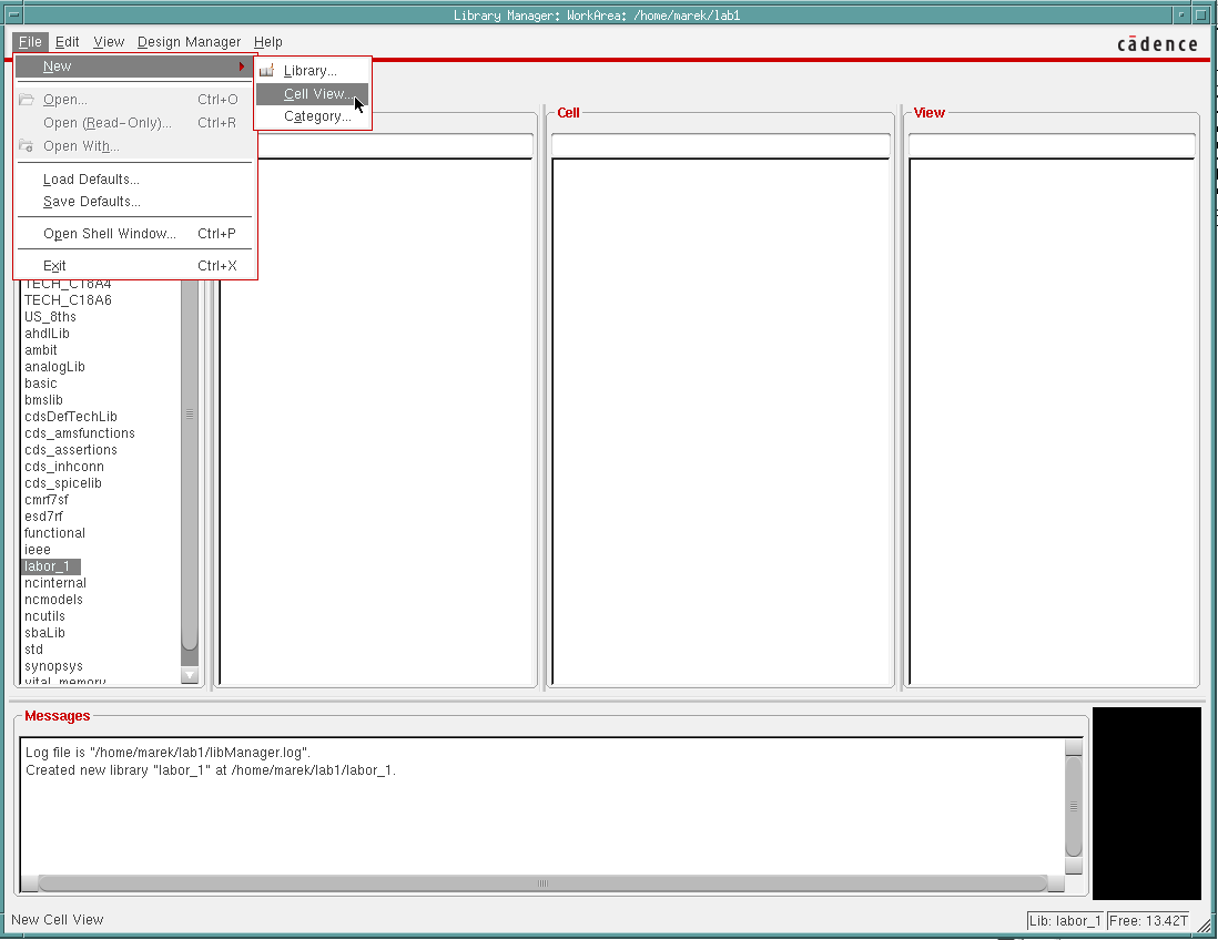

- In the window opened fill the field Cell by giving your new circuit a name, e.g. half_adder. On the images below poolsummaator is used as the name.
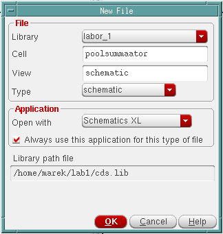
- Choose Applications->Schematics XL and select checkbox Always use this application for this type of file and press OK. As a result the schematic editor window will open.

Editing the half-adder schematic
- As a result of the previous actions we should have a schematic editor window open.
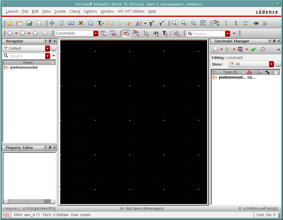

- Overview of some of the schematic shortcuts
- 'i' - instance , adding new instance of a cell to the schematic
- 'w' - wire , adding wire to the schematic for connecting elements
- 'l' - label , inserting a label on a connection
- 'p' - pin , creating a new input/output pin
- 'f' - fit to view , changes to zoom to fit the whole schematic to the view
- 'u' - undo , undo the last action
- 'X' - Check and Save' , checks the schematic and saves it
- Zooming in can be done by holding down the right mouse button and selecting an area. To leave the zoom quickly, press f
- From every insertion mode you can quickly exit by pressing ESC
- When in the wire mode, you can press s for snap functionality.
- NB! Undo works until last save. Changes made before the save can not be taken back.
Creating a sheet border and title
- Press the key i and in the opening window press Browse
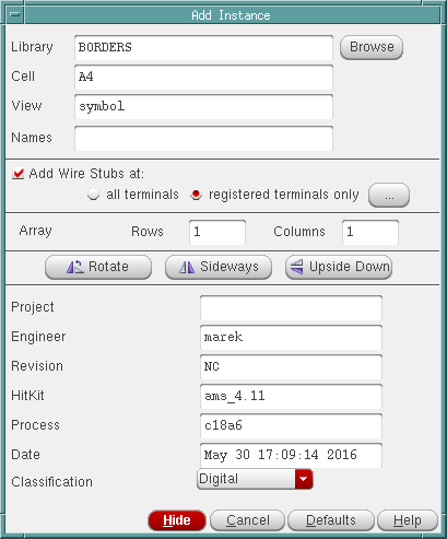
- Library Browser will open where you should navigate to Library->BORDERS->Cell->A5.
- We can close the Library Manager window by pressing Close
- Also we can hide the Add Instance window temporarily by pressing Hide

- After that the border can be placed by moving mouse in the black area of schematic editor and pressing left mouse button.
- When the border is placed, you can press f to fit the view.

Adding schematic elemenets of half-adder
- Press the key i and choose Browse
- In the Library Browser window that opened, navigate to Library->CORELIB where the schematic elements can be found.
- First of all we need to place some AND gates.
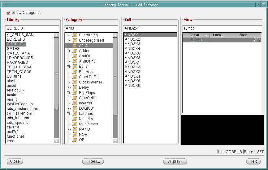
- To do that, navigate to Category->AND->Cell->AND2X1
- The numbers after the gate name show how many inputs does it have and its fan-out (number of gate inputs it can feed or connect to). In this case we have a two input AND gate with 1 fan-out.

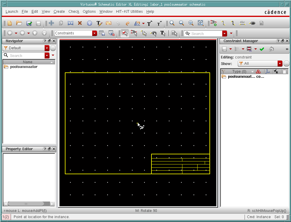
- For a half-adder we need 3 AND gates, 2 NOT gates (inverters) and 1 OR gate
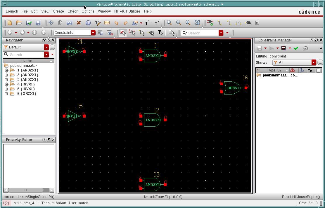

Adding inputs and outputs for the half-adder
- To add the inputs and output pins, press p
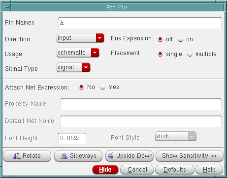
- For the first pin name choose A with direction input
- Placing pins works the same way as placing instances of cells

- For a half-adder we need two inputs (A and B) and two outputs (Sum and Carry)

Adding connections
- Press w to choose wire and by using snap, connect the elements as following:
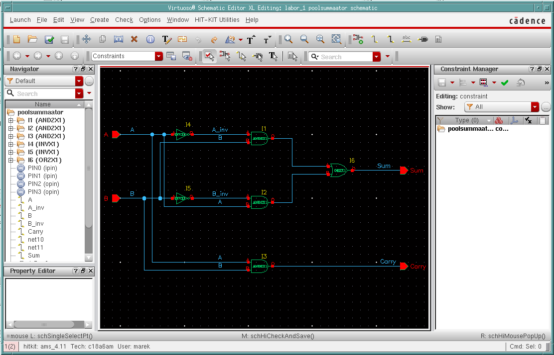
- For a better readability of the schematic you can add labels by pressing the key l.

Saving the half-adder schematic
- For saving the schematic press x
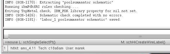
- In the Cadence main window you can check whether the saving was successful and if not, what were the errors.

Creating a symbol for the half-adder
- In order to use the newly created schematic as a component in other schematics, a symbol view must be created.
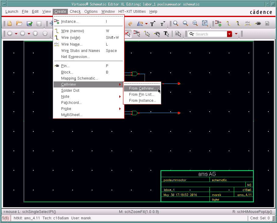
- To create a symbol, navigate from menu to Create->Cellview->From Cellview

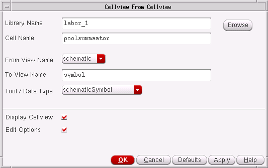
- A window will pop up, where you can simply press OK as the default options are fine at this point.

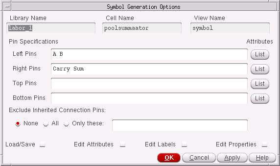
- In the following popup window you can choose the pin specifications.
- Finally continue by pressing OK

- Next, Cadence Symbol Editor will open
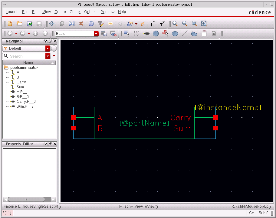
- The symbol created by default is a rectable. By using the toolbar, it can be designed as desired.

Full adder from two half-adders
- By using the finished half-adder component, we can create a full adder
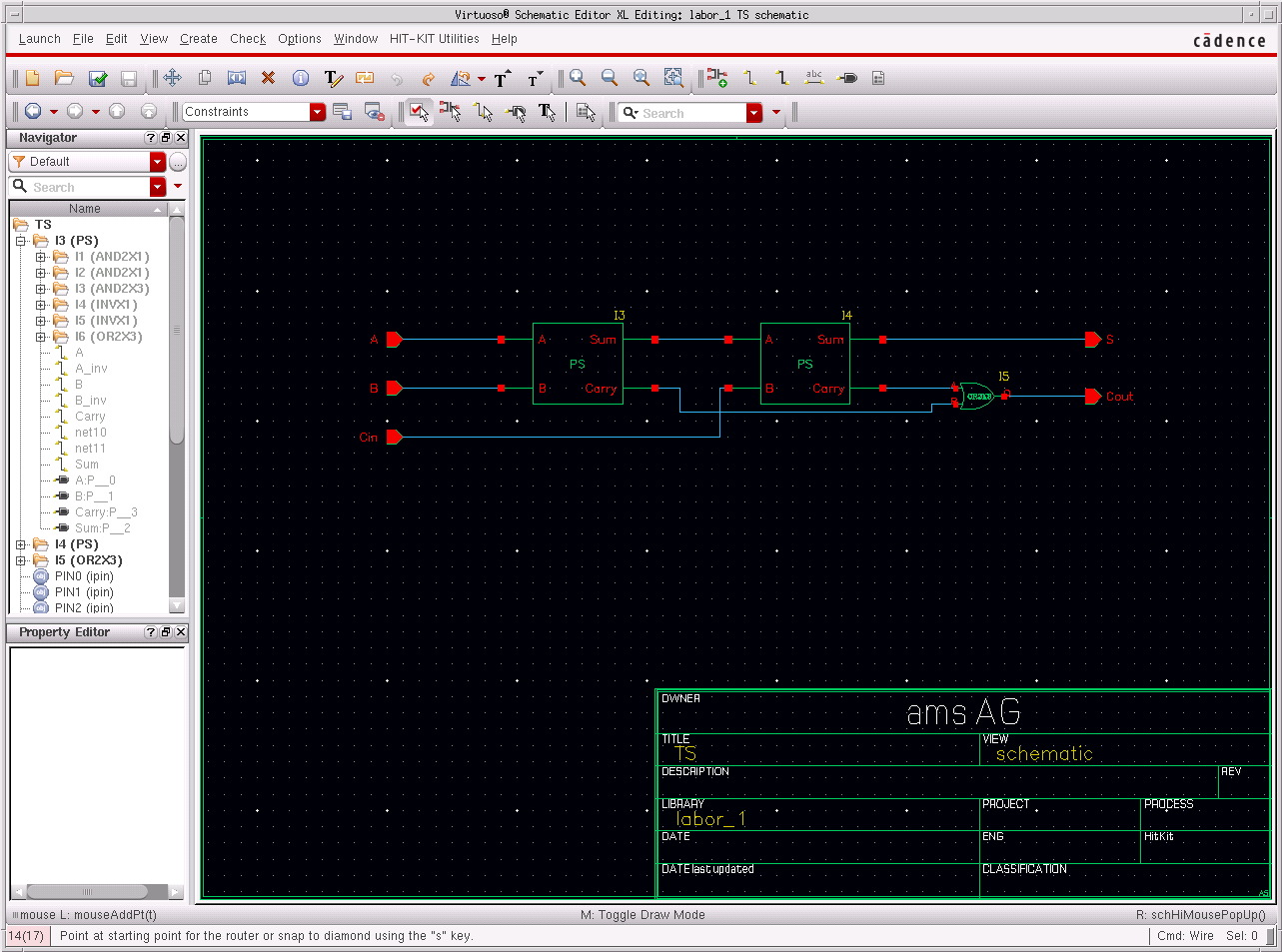
- This can be made into a symbol as well, so it can be used in other schematics as a component.

- The component can be also be opened in schematic view. To do that:
- Double click on the component symbol
- Use the command Descend Edit or its shortcut Shift+E
- To return back to last view Return command can be used or its shortcut Ctrl+E
- This can be useful for example when we need to change the fanout of the component.
- NB! when changing the component, it will change everywhere, where it has been used.
4-bit adder
- Now we should have all the components necessary for a 4-bit adder: one half-adder and three full-adders.
- Carry chain can be done serially in this schematic with Ripple Carry Adder, which is suitable for a small 4-bit adder. For bigger adders parallel carry would be recommended, e.g. Lynch-Swartzlander Spanning Tree Carry Lookahead Adder.
- For this schematic we will be using 4-bit bus.
- To make the buses more visible, we will use bold line for the connections.
- For bringing out individual bits from a bus and connecting them, labelling must be used.

4-bit adder simulation
- Now that we have finished, checked and saved the schematic design, we will proceed with simulation.
- Let us open the tool NC-Verilog
- From Cadence main window choose from menu Tools->NC-Verilog

- A new window will open where a few things should be configured
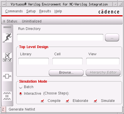
- Run Directory - press on the button with three dots (...) and choose a working directory. (In this case we should create the working directory, for example lab1_simu)
- Choose design by pressing on Browse, selecting your schematic and schematic view.


NC-Verilog initialization and settings
- Press on the first icon in the left Initialize Design

- A window will pop up where OK should be chosen.

- Configure a few parameters from Setup->Netlist
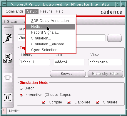

- A menu will open
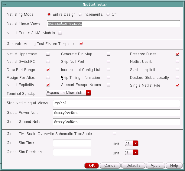
- Choose the following settings
- Netlist These Views->schematic symbol
- choose Single Netlist File
- Global Sim Time set as 1 with unit ps
- Global Sim Precision set as 1 with unit fs

- Next, choose Setup->Record Signals
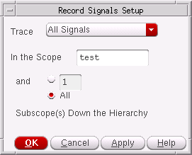
- Choose All

Creating NC-Verilog Netlist
- As a next step we should generate netlist for our schematic. For that press on the NC-Verilog main window a button Generate Netlist

- On the Cadence main window you can check whether the netlist was generated successfully without errors.

NC-Verilog simulation input data
- For the simulator to be able to simulate anything, we need input data
- For this purpose choose from NC-Verilog main window Commands->Edit Test Fixture

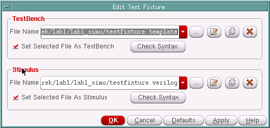
- In the opened window there are two panes: TestBench and Stimulus
- For a simple simulation, we are only interested in Stimulus section. Press there on the Edit button.

- A text editor should open with a file testfixture.verilog
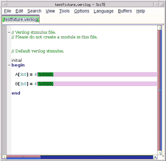
- Here you can see code generated by default that initializes the simulation.

- Now we can add our own values. 4 to 5 input number pairs, every change simulate for 10 simulation units.

- After editing, it is a good idea to check for errors. This can be done from Edit Test Fixture window with a button Check Syntax
- If everything is good, a message will be displayed

NC-Verilog Simulation
- Start the simulation by clikcing in the NC-Verilog main window, on the left side on a button Simulate
- As a result SimVision will start and two new windows will open: Console - SimVision and Design Browser = SimVision

Simulation results, SimVision
Viewing simulation results
- In the opened windows, let us focus on the Design Browser
- Here, on the left side of the window, choose -simulator-test+top
- and on the right side of the window choose inputs-outputs for which values we are interested of seeing on the waveform graph. Finally press on Send to Waveform.

- A new window will appear: Waveform - SimVision
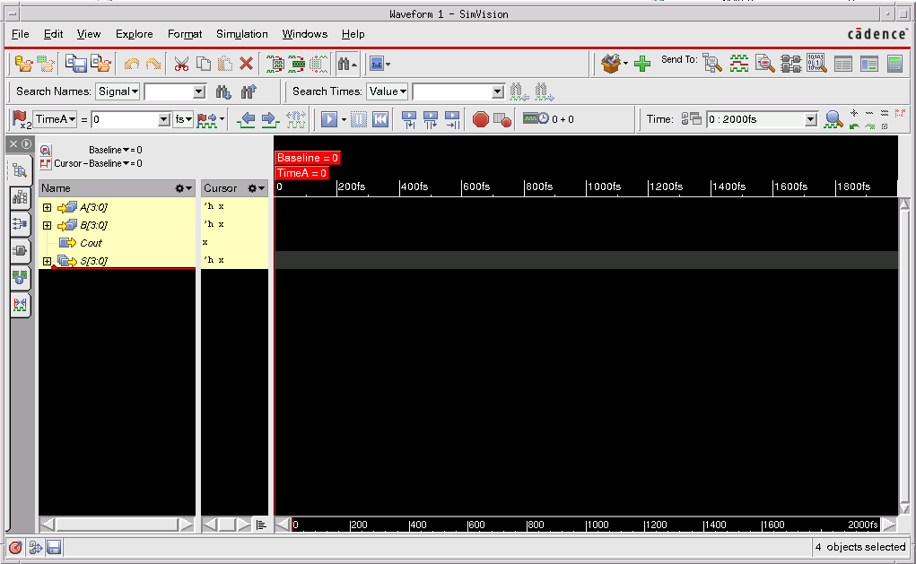

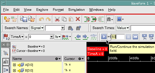
- Here, press on a triangle symbol by the Run button, so that we could edit time field.
- In the time field insert a number of simulation units, 60.
- and press Run button.

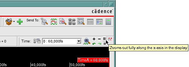
- So that we could see the whole view, the waveform should be zoomed out. Press = button on the right border of the toolbar.

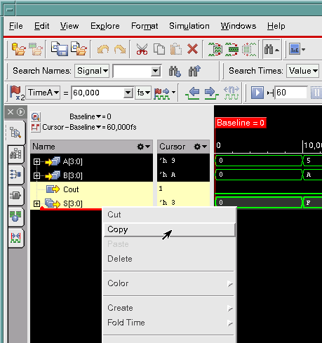
- If we have multiple outputs that are related with each other, in this case Carry signal and sum output, it is reasonable to view them together for a better readabilty.
- In order to do that simply copy these two signals - with left mouse button click on the signals while holding SHIFT key and then by clicking right mouse button, choose Copy from the menu.
- Finally paste the signals down below, by clicking again with the right mouse button on the black background and choose Paste

- Afterwards choose the copied signals and by pressing again on the right mouse button choose Create->Bus from the menu.

Simulation results
- Now we can easily follow the waveform and check the results of the adder