CPUProject
CPU project is one of the projects designed in department of computer engineering at TTU as a lab project. The main aims of this project are:
- Developing a generic simple CPU
- Writing a compiler for it
- Compiling GCC for this architecture
- Booting a lightweight linux on it
This project has many different aspects and each of these aspects can be used for laboratories in different courses.
Contents
- 1 CPU Design
- 2 Assembler
- 3 Compiler
CPU Design
Functionality Requirements
The CPU is supposed to be able to perform the following operations:
- Addition/Subtraction
- Increment/Decrement
- Arithmetic and Logical Shift and Rotate through carry
- Bitwise AND, OR, XOR and NOT
- Negation
- Load/Store
- Unconditional Branch (jump)
- Branch if zero / Branch if Overflow / Branch if Carry/ Branch if Equal
- Clear Registers/Flags
- PUSH / POP
- NOP/HALT
It can use these operations to build more sophisticated operations later.
Architecture
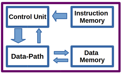
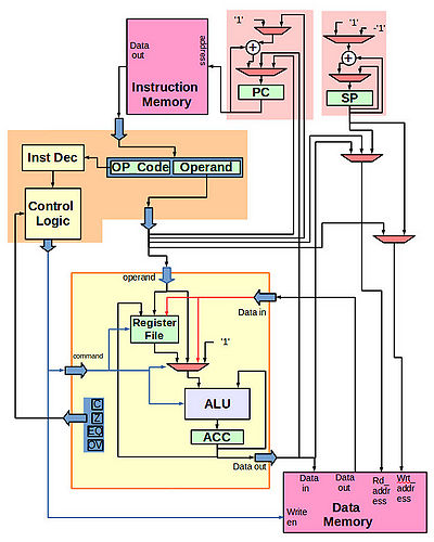
The architecture of this CPU is based on harvard architecture which has separate instruction and data memory. The instructions are assumed to be in the instruction memory before boot.
Instruction Format
Our CPU's instuction has 8 bit of upcode and one operand that can be as long as 32 bit. First 2 bits of OPcode are at the moment reserved.
Addressing Modes
The following Addressing modes are supported in out processor:
- direct: program counter jumps to an address directly provided to it through instruction's operand
- relative: the program counter will jump to a location reletive to its current location
- indirect: program counter will jump to an address stored in a memory location
- register: program counter will jump to an address stored in a register
- indexed: program counter will jump to an address stored in the memory with address stored in a register
Instruction Set (IS)
The following instrcutions designed for the CPU:
| Instruction | Register Transfer Language | OpCode | DPU Command | Data To DPU | MemAddress | Next PC | |
|---|---|---|---|---|---|---|---|
| 1 | Add_A_B | A <-- A + B | 00 0000 | 00 000 0000 10 | ---- | ---- | PC_out+1 |
| 2 | Add_A_Mem | A <-- A + Mem[Operand] | 00 0001 | 00 000 0000 00 | ---- | Operand | PC_out+1 |
| 3 | Add_A_Dir | A <-- A + Operand | 00 0010 | 00 000 0000 01 | Operand | ---- | PC_out+1 |
| 4 | Sub_A_B | A <-- A - B | 00 0011 | 00 000 0001 10 | ---- | ---- | PC_out+1 |
| 5 | Sub_A_Mem | A <-- A - Mem[Operand] | 00 0100 | 00 000 0001 00 | ---- | Operand | PC_out+1 |
| 6 | Sub_A_Dir | A <-- A - Operand | 00 0101 | 00 000 0001 01 | Operand | ---- | PC_out+1 |
| 7 | IncA | A <-- A + 1 | 00 0110 | 00 000 0000 11 | ---- | ---- | PC_out+1 |
| 8 | DecA | A <-- A - 1 | 00 0111 | 00 000 0001 11 | ---- | ---- | PC_out+1 |
| 9 | ShiftArithR | A <-- A(7) & A(7 downto 1) | 00 1000 | 00 000 0111 00 | ---- | ---- | PC_out+1 |
| 10 | ShiftArithL | A <-- A(7) & A(5 downto 0)& '0' | 00 1001 | 00 000 1000 00 | ---- | ---- | PC_out+1 |
| 11 | ShiftA_R | A <-- A(6 downto 0)& '0' | 00 1010 | 00 000 1010 00 | ---- | ---- | PC_out+1 |
| 12 | ShiftA_L | A <-- '0' & A(7 downto 1) | 00 1011 | 00 000 1011 00 | ---- | ---- | PC_out+1 |
| 13 | RRC | A <-- C & A(7 downto 1) ,C<-- A(0) | 00 1100 | 00 000 1110 XX | ---- | ---- | PC_out+1 |
| 14 | RLC | A <-- A(6 downto 0) & C ,C<-- A(7) | 00 1101 | 00 000 1111 XX | ---- | ---- | PC_out+1 |
| 15 | And_A_B | A <-- A and B | 00 1110 | 00 000 0100 10 | ---- | ---- | PC_out+1 |
| 16 | OR_A_B | A <-- A or B | 00 1111 | 00 000 0101 10 | ---- | ---- | PC_out+1 |
| 17 | XOR_A_B | A <-- A xor B | 01 0000 | 00 000 0110 10 | ---- | ---- | PC_out+1 |
| 18 | FlipA | A <-- not (A) | 01 0001 | 00 000 1100 00 | ---- | ---- | PC_out+1 |
| 19 | NegA | A <-- not(A) + 1 | 01 0010 | 00 000 1001 00 | ---- | ---- | PC_out+1 |
| 20 | Jmp | PC <-- Operand | 01 0011 | 00 000 0010 XX | ---- | ---- | Operand |
| 21 | JmpZ | if Z = 1: PC <-- Operand | 01 0100 | 00 000 0010 XX | ---- | ---- | if Z=1 then Operand else PC_out+1 |
| 22 | JmpOV | if OV = 1: PC <-- Operand | 01 0101 | 00 000 0010 XX | ---- | ---- | if OV=1 then Operand else PC_out+1 |
| 23 | JmpC | if C = 1: PC <-- Operand | 01 0110 | 00 000 0010 XX | ---- | ---- | if C=1 then Operand else PC_out+1 |
| 24 | Jmp_rel | PC <-- PC + Operand | 01 0111 | 00 000 0010 XX | ---- | ---- | PC <-- PC + Operand |
| 25 | JMPEQ | if EQ = 1: PC <-- Operand | 01 1000 | 00 000 0010 XX | ---- | ---- | if EQ=1 then Operand else PC_out+1 |
| 26 | ClearZ | Z <--- 0 | 01 1001 | 00 001 0010 XX | ---- | ---- | PC_out+1 |
| 27 | ClearOV | OV <--- 0 | 01 1010 | 00 010 0010 XX | ---- | ---- | PC_out+1 |
| 28 | ClearC | C <--- 0 | 01 1011 | 00 100 0010 XX | ---- | ---- | PC_out+1 |
| 29 | ClearACC | ACC <-- 0 | 01 1100 | 00 000 1101 XX | ---- | ---- | PC_out+1 |
| 30 | LoadPC | PC <---- A | 01 1101 | 00 000 0010 XX | ---- | ---- | A |
| 31 | SavePC | A <---- PC | 01 1110 | 00 000 0011 01 | PC | ---- | PC_out+1 |
| 32 | Load_A_Mem | A <-- Mem[Operand] | 01 1111 | 00 000 0011 00 | ---- | Operand | PC_out+1 |
| 33 | Store_A_Mem | Mem[Operand] <-- A | 10 0000 | 00 000 0010 XX | ---- | Operand | PC_out+1 |
| 34 | Load_B_Dir | B <-- Operand | 10 0001 | 01 000 0010 XX | Operand | ---- | PC_out+1 |
| 35 | Load_B_Mem | B <-- Mem[Operand] | 10 0010 | 11 000 0010 XX | ---- | Operand | PC_out+1 |
| 36 | Load_A_B | A <-- B | 10 0011 | 00 000 0011 XX | ---- | ---- | PC_out+1 |
| 37 | Load_B_A | B <-- A | 10 0100 | 10 000 0010 XX | ---- | ---- | PC_out+1 |
| 38 | Load_Ind_A | A <-- M[A] | 10 0101 | 00 000 0011 00 | ---- | A | PC_out+1 |
| 39 | PUSH | Mem [0 + SP] <--- A,SP <--- SP + 1 | 11 1100 | 00 000 0010 XX | ---- | SP | PC_out+1 |
| 40 | POP | A <--- Mem [0 + SP - 1],SP <--- SP - 1 | 11 1101 | 00 000 0011 00 | ---- | SP - 1 | PC_out+1 |
| 41 | NOP | NOP | 11 1110 | 00 000 0010 XX | ---- | ---- | PC_out+1 |
| 42 | HALT | HALT | 11 1111 | 00 000 0010 XX | ---- | ---- | PC |
Implementation of complex instructions
the follwoing instructions can be also implemented with the ones in IS:
- Call "function_name":
PUSH
SavePC
Push
Jmp "function address"
POP
- Return:
POP
Add_A_Dir 4
LoadPC
- IndJMP "MemAddress":
PUSH
Load_A_Mem "MemAddress"
LoadPC
Note: its important to POP back the ACC value on the jump destination.
- JmpB:
PUSH
Load_A_B
LoadPC
Note: its important to POP back the ACC value on the jump destination.
- JmpIndx:
PUSH
Load_Ind_A
LoadPC
Note: its important to POP back the ACC value on the jump destination.
DataPath unit
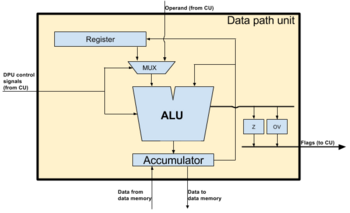
Datapath unit includes an Arithmatic Logical Unit (ALU), one Accumulator(ACC) and one general purpose register(Register B) and 2 multiplexers along with the flags (see Fig. 3). The DPU command is formed as following:
ALU Multiplexer
The ALU multiplexer chooses the inputs according to the table 2.
| command | output | |
|---|---|---|
| 1 | 00 | MemDATA |
| 2 | 01 | ControlDATa |
| 3 | 10 | B |
| 4 | 11 | 1 |
B-Register Multiplexer
The B-register multiplexer chooses the inputs according to the table 3.
| command | output | |
|---|---|---|
| 1 | 00 | B |
| 2 | 01 | ControlDATa |
| 3 | 10 | ALUResult |
| 4 | 11 | MemDATA |
ALU
The ALU covers the following operations:
| Command | Operation | Description | |
|---|---|---|---|
| 1 | 0000 | A + B | Addition |
| 2 | 0001 | A - B | subtraction |
| 3 | 0010 | A | Bypass A |
| 4 | 0011 | B | Bypass B |
| 5 | 0100 | A AND B | bitwise And |
| 6 | 0101 | A OR B | bitwise OR |
| 7 | 0110 | A XOR B | bitwise XOR |
| 8 | 0111 | '0' & A(BITWIDTH-1 DOWNTO 1) | Logical Shift Right |
| 9 | 1000 | A(BITWIDTH-2 DOWNTO 0) & '0' | Logical Shift Left |
| 10 | 1001 | NOT(A) + 1 | Negation |
| 11 | 1010 | A(BITWIDTH-1) & A(BITWIDTH-1 DOWNTO 1) | Arithmetic Shift Right |
| 12 | 1011 | A(BITWIDTH-1) & A(BITWIDTH-3 downto 0)& A(0) | Arithmetic Shift Left |
| 13 | 1100 | NOT(A) | Flip |
| 14 | 1101 | 0 | Clear A |
| 15 | 1110 | Cflag & A(BITWIDTH-1 downto 1) | Rotate Right Through Carry |
| 16 | 1111 | A(BITWIDTH-2 downto 0)& Cflag | Rotate Left Through Carry |
For addition/subtraction a ripple carry model is made out of chain of full adders.
Flags
| command | FlagToClear | |
|---|---|---|
| 1 | 001 | Clear Z |
| 2 | 010 | Clear OV |
| 3 | 100 | Clear C |
In DPU has the following flags:
- Zero Flag (Z): will be set if the result of the operation is zero
- Overflow Flag (OV): will be set if an overflow happens in signed operations (as an example if we have 8 bit addition of 82+91 the answer we expect is 173 but the result would be interpreted as -45). Overflow flag can be realized in the following way:
- Carry Flag (C): will be set if the unsigned addition or subtraction results in a carry.
- Equal Flag (EQ): will be set if ACC value is equal to the operand
To clear flags,the SetFlag commands are used in DPU command (see table 5).
Instruction Memory (ROM)
Instruction memory is a read only memory that user will fill in the beginning.
Data Memory
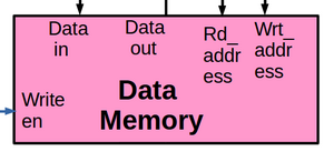
Data memory is made out of blocks of 1024 registers. If user wants bigger size memory, it would be necessary to add more blocks. Writing into data memory takes one clock cycle but readingf from it can be done instantly(or in reletively shorter time). So we can assume that if we issue address in one clock cycle, we can get the data in the same clock cycle. There is a stack is at the top of data memory and its size is not restricted. Behavioural VHDL description of one instance of data memory is shown in the code below.
Control unit
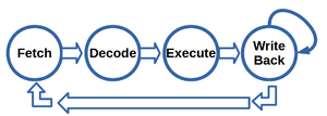
Control unit has four states:
- Fetch: fetches the instructions from instruction memory and loads it in Instruction Register (IR). DPU is IDLE. No Read from data memory.
- Decode: decodes the information in IR. DPU is IDLE. No Read from data memory.
- Execute: if execution on DPU is needed the proper control signals would be provided, otherwise DPU will stay IDLE. Read from data memory performed if needed.
- WriteBack: in case there is a need to write a data into memory it will happen in this stage. All changes in Program Counter(PC) is happening here so all conditional and unconditional branching would be decided in this state. in case the instruction is HALT the PC would be frozen.
VHDL complete versions
- 8-bit Version (17 dec 2014)
- 16-bit Version
- 32-bit Version
Functional Testing
Following machine code program has been made to test functionality of all instructions. The test program doesnt cover all the cases but run through all the instructions. (at the moement not all the instructions are covered-12% missing)
Load_B_Dir "00011000"
OR_A_B
IncA
Sub_A_B
NOP
JmpC "00001000"
NOP
NOP
RRC
RLC
NOP
ClearC
Store_A_Mem  "00010000"
PUSH
SavePC
PUSH
Jump "00010101"
POP
ShiftArithL
DecA
HALT
Load_A_Mem "00010000"
And_A_B
JmpZ "00011001"
NOP
ClearZ
Add_A_Mem "00010000"
Sub_A_Mem "00010000"
Add_A_B
Sub_A_Dir "00001100"
FlipA
XOR_A_B
NegA
ShiftArithR
ShiftA_L
ShiftA_R
ClearACC
POP
Add_A_Dir  "00000011"
LoadPC
HALT
Synthesizing and implementation on FPGA
One of the parts of this project is to synthesize 8-bit version of CPU on an FPGA board. "Nexsys 3" board from Digilent has been chosen for implementation. Clock source is controllable via a switch on the board. ClK would be either the 100MHz on-board oscillator or generated signal from one push button (for debugging). The Accumulator value will be displayed on Seven-Segments and the flag values will be displayed on the LEDs.
You need the following files along the CPU VHDL files for synthesis on and implementation on FPGA:
- Top-level Entity: TopLevel.vhd
- Denouncing circuit: Debouncer.vhd
- Seven-segment Decoder: SevenSegment.vhd
The User Constraint File (UCF)
The following is the user constraints file for the project:
NET clk LOC = V10;
NET rst LOC = C4;
NET ClkBttn LOC = D9;
NET ClockSrc LOC = T10;

NET FlagOutput<0> LOC = U16;
NET FlagOutput<1> LOC = V16;
NET FlagOutput<2> LOC = U15;
NET FlagOutput<3> LOC = V15;

NET SevenSeg<6> LOC = T17;
NET SevenSeg<5> LOC = T18;
NET SevenSeg<4> LOC = U17;
NET SevenSeg<3> LOC = U18;
NET SevenSeg<2> LOC = M14;
NET SevenSeg<1> LOC = N14;
NET SevenSeg<0> LOC = L14;

NET AN<3> LOC = P17;
NET AN<2> LOC = P18;
NET AN<1> LOC = N15;
NET AN<0> LOC = N16;
Future plans
The following are the future plans for CPU:
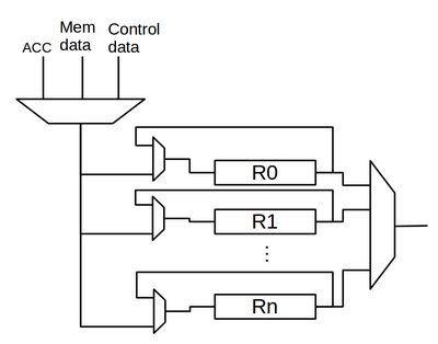
- Adding a couple of general purpose registers. maybe in this configuration:
in this case we need a decoder to generate contorl signals for input multiplexers so only one mux can get input from outside at any given time.
- implement barrel shift on acc
- Adding I/O
- first try would be Input and Output registers
- wishbone bus maybe?
- Adding interupts + super user mode (motorla has it MC68K)?
- Pipelining
- Branch prediction
- Synthesis and FPGA implementation
- VGA controller?
- UART implementation
- implementation of Timers/Counters and peripherals
- Direct Memory Access (DMA)
- Memory management unit (MMU)
Assembler
Python Assembly translator
A simple assembly translator was designed to make debugging process faster. Here you can see 32 bit version of the code:
import re
InstructionOpCode = {

                'Add_A_B':	"000000",
                'Add_A_Mem': 	"000001",
                'Add_A_Dir': 	"000010",
                'Sub_A_B':	"000011",
                'Sub_A_Mem':	"000100",
                'Sub_A_Dir': 	"000101",

                'IncA': 	"000110",
                'DecA':		"000111",

                'ShiftArithR':	"001000",
                'ShiftArithL':	"001001",
                'ShiftA_R':	"001010",
                'ShiftA_L':	"001011",
                'RRC':	  	"001100",
                'RLC':		"001101",

                'And_A_B':	"001110",
                'OR_A_B':	"001111",
                'XOR_A_B':	"010000",
                'FlipA':	"010001",
                'NegA':		"010010 ",

                'Jump':		"010011",
                'JmpZ':		"010100",
                'JmpOV':	"010101",
                'JmpC':		"010110",
                'Jmp_rel':	"010111",
                'JMPEQ':	"011000",

                'ClearZ':	"011001",
                'ClearOV':	"011010 ",
                'ClearC':	"011011",
                'ClearACC':	"011100",

                'LoadPC': 	"011101",
                'SavePC':	"011110",

                'Load_A_Mem':	"011111",
                'Store_A_Mem':	"100000",
                'Load_B_Dir':	"100001",
                'Load_B_Mem':	"100010",

                'Load_A_B':	"100011",
                'Load_B_A':	"100100",
                'Load_Ind_A ':	"100101",

                'PUSH':		"111100",
                'POP':		"111101",
                'NOP':		"111110",
                'HALT':		"111111",

}
AssemblyFile = open('Assembly.txt', 'r+')
MachineCodeFile = open('MachineCode.txt', 'w')
counter=0
for line in AssemblyFile:

    for key in InstructionOpCode:
        if key in line:
            operand= "00000000"
            if "Mem" in line:
                operand = re.findall(r'\d+',line)[0]
            elif "Jmp" in line:
                operand = re.findall(r'\d+',line)[0]
            elif "Dir" in line:
                operand = re.findall(r'\d+',line)[0]
            operand = "00000000"+"00000000"+"00000000"+ operand
            MachineCodeFile.write(str(counter)+ " =>   "+ "\"00"+InstructionOpCode[key]+operand+'\",'+'\n')
            counter +=1

MachineCodeFile.close()
AssemblyFile.close()
Java Assembler
This Assembler is wrote by Karl Janson as a project during system modeling course. You can find the information about how to use it in the User Manual.
Downloads
- Executable File:
- The Assembler code: File:picoAssembler.zip
- Assembler Intructions File: File:intructions.txt
Note: Codes and User Manual for the assembler are placed in the Public Domain with the authorization of its author, Karl Janson.
