Pico CPU:
Writing the behaviour Model
Introduction
In this lab you will write a behavioral model of an 8-bit CPU with stack and conditional jumps etc. in VHDL, based on the Instruction Set Architecture provided to you in this manual. the general idea of this lab is shown in the fig bellow: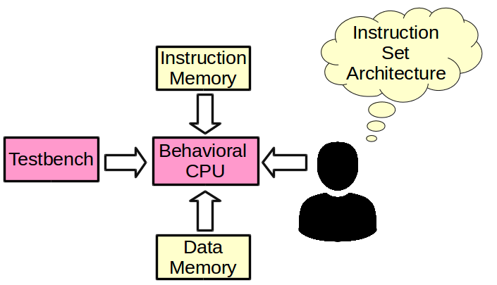
All parts in yellow are provided to you and all the red blocks should be written by you. The program is hard coded into the instruction memory. you need to write a testbench that provides the CPU with clock etc. to run this program to the end. Please make sure that you have read the preliminary readings! you can find it in the related readings tab on the left.
Hack and Slash CPU Design
General Information
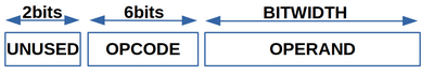
The instruction for our CPU has the following format:
please note that:
- You need to have at least 8 general purpose registers in a register file in your CPU.
- You should implement a stack at the top of your data memory
- Fetch: in this phase, we processor fetches an instruction (according to program counter)from instruction memory and writes it in Instruction Register
- Decode: fetched instruction Op-Code will be decoded and data or address will be extracted
- Execution: data will be fed to Datapath Unit and instruction will be executed
- Write-Back: the result of the operation will be written to Data Memory
Instruction Set Architecture
Here is the instruction set architecture for your CPU:
| # | Instruction | Register Transfer Language |
| 1 | Add_A_R operand | A < -- A + R(operand) |
| 2 | Add_A_Mem Operand | A < -- A + Mem[Operand] |
| 3 | Add_A_Dir Operand | A < -- A + Operand |
| 4 | Sub_A_R Operand | A < -- A - R(operand) |
| 5 | Sub_A_Mem Operand | A < -- A - Mem[Operand] |
| 6 | Sub_A_Dir Operand | A < -- A - Operand |
| 7 | IncA | A < -- A + 1 |
| 8 | DecA | A < -- A - 1 |
| 9 | ShiftArithR | A < -- A(7) & A(7 downto 1) |
| 10 | ShiftArithL | A < A(7) & A(5 downto 0)& '0' |
| 11 | ShiftA_R | A < -- '0' & A(7 downto 1) |
| 12 | ShiftA_L | A < -- A(6 downto 0)& '0' |
| 13 | RRC | A < -- C & A(7 downto 1) ,C< -- A(0) |
| 14 | RLC | A < -- A(6 downto 0) & C ,C< -- A(7) |
| 15 | And_A_R | A < -- A and R(operand) |
| 16 | OR_A_R | A < --A or R(operand) |
| 17 | XOR_A_R | A <-- A xor R(operand) |
| 18 | FlipA | A <-- not (A) 0 |
| 19 | NegA | A <-- not(A) + 1 |
| 20 | Jmp Operand | PC <-- Operand |
| 21 | JmpZ Operand | if Z = 1: PC <-- Operand |
| 22 | JmpOV Operand | if OV = 1: PC <-- Operand |
| 23 | JmpC Operand | if C = 1: PC <-- Operand |
| 24 | Jmp_rel Operand | PC <-- PC + Operand |
| 25 | JMPEQ Operand | if EQ = 1: PC <-- Operand |
| 26 | ClearZ | Z <- 0 |
| 27 | ClearOV | OV <- 0 |
| 28 | ClearC | C <- 0 |
| 29 | ClearACC | ACC < 0 |
| 30 | LoadPC | PC <-- A |
| 31 | SavePC | A <-- PC |
| 32 | Load_A_Mem | A <-- Mem[Operand] |
| 33 | Store_A_Mem | Mem[Operand] <-- A |
| 34 | Load_R0_Dir | R0 <-- Operand |
| 35 | Load_R0_Mem | R0 <-- Mem[Operand] |
| 36 | Load_A_R | A <-- R(operand) |
| 37 | Load_R_A | R(operand) <-- A |
| 38 | Load_Ind_A | A <-- M[A] |
| 39 | PUSH | Mem [0 + SP] <-- A,SP <-- SP + 1 |
| 40 | POP | A <-- Mem [0 + SP - 1],SP <-- SP - 1 |
| 41 | NOP | NOP |
| 42 | HALT | HALT |
Memories
We provide the Memories for your CPU. The code that we are interested in, is hard coded into your ROM (Instruction Memory).Tasks
- write a behavioral CPU that complies with the above mentioned ISA.
- write a testbench that executes the code in the instruction memory.
- write a report about how you did it.
Related Readings