PicoCPU
The picoCPU was built as a course work during the Digital Systems Modelling and Synthesis course. Its goal is to provide very simple and minimal, but still functional, general purpose CPU design for educational purposes.
Contents
Architecture
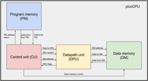
PicoCPU is divided into four main components (seen in the figure on the right):
- Control Unit (CU): Reads the instructions, advances the program counter and controls the work of the rest of the CPU
- Data Path Unit (DPU): Does all the calculations and other data manipulation operations
- Program Memory (PM): A ROM that contains the program data. In picoCPU, it is emulated by the testbench.
- Data memory (DM): The data memory is implemented as a RAM. It contains the temporary data that are needed by the currently running program.
PicoCPU is designed to have a generic design and it's bitwidth is scalable to satisfy the user's preference, being 8-bit by default. All the data are always treated as signed values.
Control Unit
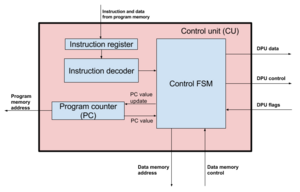
The most important part of the CU is the control FSM, that has four states:
- Fetch: fetches the data from the program memory and stores it in the instruction register.
- Decode: Seperates operand from instruction
- Execute: Executes the instruction
- Write back: Writes execution result to the destination register or memory address, advances the program counter.
The program counter (PC) is a pointer to the program memory address of the currently executed instruction. The program counter's value directly specifies the memory address for reading the program memory. Usually, the program counter is increased by one after the current instruction is loaded (next address of the program memory is chosen). However, it is also possible to change the PC's value to an arbitrary one, for example to implement branching in the code.
Data Path Unit
ALU
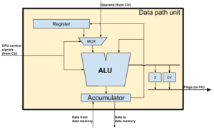
The central part of the DPU is the Arithmetic and Logic Unit (ALU). ALU's task is to execute all the arithmetical and logical calculations. It has many functions and the correct one is chosen by the CU, based on the currently executed instruction. Every calculation result always ends up in the accumulator register. The first input of the ALU can be multiplexed between a register and the operand from the operand from the program memory and the contents of a register (the multiplexer can be controlled be specific instructions). The second input is always the contents of the accumulator.
Memory operations
Writing to and reading from the data memory always involves the accumulator - all data read from the memory always ends up in the accumulator. It is also only possible to write into the memory data that is stored in the accumulator.
For writing into the register, the file data to be written has to be already in the accumulator. Then, a special instruction is used for doing the writing. Reading from the register can be done only through the ALU, using the regular ALU-related instructions, just the MUX has to be configured to take its input from the register. Due to the fact that it is possible to access the register only through the ALU, the value of the register can only be retrieved by running an arithmetic or logic operation on it. If just retreaving of the value is desired, a neutral operation, that does not change the value can be performed, like adding or subtracting 0 to/from the register or AND-ing the value with 1-s.
Flags
The picoCPU features two flags: zero (Z) and overflow(OV)
The zero flag indicates that the value in the accumulator is equal to 0 and OV flag indicates that the last operation caused an overflow in the accumulator. User can access the values of these flags using some conditional branching functions (BranchIfZero, etc.). The flags are only held up as long as the condition for a flag is true (i.e. the accumulator is zero) and are, thus, usually available only to the next isntruction (except some neutral instructions like NOP, that are not data-related).
Impementation
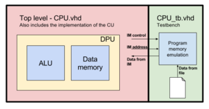
Each main component of picoCPU is implemented as a separate entity. The structure of the connections can be seen in the figure on the right.
In case of picoCPU, the program memory is emulated be the testbench. Its contents are read from a text file. This enables easy reprogramming of picoCPU for simulation purposes.
Program Memory Data format
As it can be seen in the figure on the right, each instruction for the picoCPU consists of 16 bits. The three highest bits are reserved and not currently used, so they should be given the values '0'. The next 5 bits (bits 12 - 8) specify the opcode. Finally the lowest 8 bits (bits 7-0) specify the operand. It has to be noted, that picoCPU accepts only one operand in an instruction. In case no operand is needed for the instruction, the operand bits are ignored.
Program memory file format
As mentioned above, the program memory in picoCPU is emulated by the tesbench and its contents are read from a text file. The format of the text file is quite simple: each line represents one memory address, line 1 mapping to memory address 0x0, line 2 to address 0x1 and so on. Each line contains 16 bits in a format mentioned above.
The execution of the program starts from memory address 0x0 and the address is normally increased by one after executing of every line, except branching instructions, that can cause the program execution to jump to other addresses.
Instruction set
== Table of instructions ==
| Opcode | Instruction | Description | Register Transfer Language Description |
| 00000 | ADD | Add the operand to the AC, no carry in | AC ← AC + OP |
| 00001 | SUB | Subtract the operand from the AC, no carry in | AC ← AC – OP |
| 00010 | INC | Increment the AC by one, no carry in | AC ← AC + 1 |
| 00011 | DEC | Decrement the AC by one, no carry in | AC ← AC -1 |
| 00100 | SLL | Logical shift the AC value to the left | AC ← SLL(AC) |
| 00101 | SRL | Logical shift the AC value to the right | AC ← SRL(AC) |
| 00110 | SLA | Arithmetical shift the AC value to the left | AC ← SLA(AC) |
| 00111 | SRA | Arithmetical shift the AC value the right | AC ← SRA(AC) |
| 01000 | AND | AND the operand with the AC | AC ← AC AND OP |
| 01001 | OR | OR the operand with the AC | AC ← AC OR OP |
| 01010 | XOR | XOR the operand with the AC | AC ← AC XOR OP |
| 01011 | INV | Invert the AC value | AC ← INV(AC) |
| 01100 | NEG | Calculate the opposite-signed value of the AC value (pos → neg, neg → pos) | AC ← INV(AC)+1 |
| 01101 | LOADN | Load the number in operand into the AC | AC ← OP |
| 01110 | LOADV | Load the value of the address specified in the operand into the AC | AC ← M(OP) |
| 01111 | STORE | Store the contents of the AC into the address in the operand | M[OP] ← AC |
| 10000 | JMP | Set the program counter to the value in the operand | PC ← OP |
| 10001 | BIZ | If 0 flag is set, set PC to address in operand, else by increase it by 1 | if (Z == 1) then PC ← OP, else PC ← PC +1 |
| 10010 | BINE | Subtract the operand from the AC. if 0 flag set, PC=PC+1( instruction PC+1 has to contain jump command to branch), else PC=PC+2 | AC ← AC – OP; if (Z != 1) then PC ← PC + 1, else PC ← PC + 2 |
| 10011 | BIOF | If OV flag is set, set PC to address in operand, else by increase it by 1 | if (OV == 1) then PC ← OP, else PC ← PC +1 |
| 10100 | SETR | Copy the value in the AC into the register | R ← AC |
| 10101 | CLRR | Clear the register | R ← 0 |
| 10110 | SETF | Set the flag described in operand | F[OP] ← 1 |
| 10111 | CLRF | Clear the flag in operand | F[OP] ← 0 |
| 11000 | MUXR | Set the ALU input to the register After executing that instruction, all operands in all instructions will be replaced by the contents of the chosen register until MUXOP is executed | OP ← R |
| 11001 | MUXOP | Set the ALU input to operand in. The operand in this command is ignored | OP ← OP |
| 11010 | LOADA | Load the value from a memory cell specified in the AC into the AC | AC ← M(AC) |
| 11011 | STOREA | Stores the value in the register to address in AC | M(AC) ← R |
| 11100 | HALT | Halt the CPU | PC ← PC |
| 11101 | NOP | No operation | PC ← PC + 1 |
| 11110 | NOP | All unused instructions are treated as NOP | PC ← PC + 1 |
| 11111 | NOP | All unused instructions are treated as NOP | PC ← PC + 1 |
Legend:
- AC Accumulator register
- R Register
- F Flag
- M Memory
- OP Operand
- PC Program counter
- OV Overflow flag
- Z Zero flag
- C Carry flag
Download
PicoCPU is available in a git repositori, that can be accessed from here.
It should be noted, that the same repository also contains the assembler (picoASM) and a simple higher level language compiler for picoCPU called picoLang.
In the picoCPU-s folder, there are two other folders:
- Implementation: It contains VHDL code for the picoCPU, testbenches for testing individual components and the main testbench cpu_tb.vhd, that is used for running programs on the picoCPU. It also contains the "simulation configuration" folder, which as name says, contains the configurationfiles for the simulations. For simulating the entire picoCPU, the file cpu_simu.wcfg can be used.
- asm: This folder contains the assembler files for testing different functionalities of picoCPU.


